Ultrasonic pcb cleaning
Benefits Of Ultrasonic PCB Cleaning For Electronics Manufacturing
Ultrasonic PCB cleaning has emerged as a pivotal process in the realm of electronics manufacturing, offering a multitude of benefits that enhance the quality and reliability of printed circuit boards (PCBs).
This advanced cleaning technique employs high-frequency sound waves to create microscopic cavitation bubbles in a cleaning solution. When these bubbles collapse, they generate intense localized pressure and temperature, effectively dislodging contaminants from the intricate surfaces and crevices of PCBs. Consequently, the adoption of ultrasonic cleaning in electronics manufacturing has become increasingly prevalent due to its numerous advantages.
One of the primary benefits of ultrasonic PCB cleaning is its unparalleled efficiency in removing contaminants.
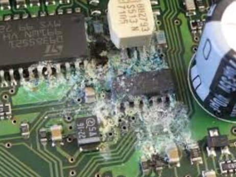
Traditional cleaning methods, such as manual scrubbing or spray washing, often fall short in reaching the minute spaces between components and under surface-mounted devices. In contrast, ultrasonic cleaning ensures thorough penetration of the cleaning solution into these hard-to-reach areas, thereby eliminating flux residues, solder paste, dust, and other particulate matter that can compromise the functionality of the PCB. This comprehensive cleaning capability is crucial for maintaining the integrity and performance of electronic devices, particularly in high-reliability applications such as aerospace, medical devices, and telecommunications.
Moreover, ultrasonic PCB cleaning significantly reduces the risk of damage to delicate components.
Manual cleaning methods can exert physical stress on the PCB, potentially leading to mechanical damage or dislodging of small parts. Ultrasonic cleaning, however, is a non-contact process that minimizes the likelihood of such damage. The gentle yet effective action of cavitation bubbles ensures that even the most fragile components are cleaned without being subjected to undue force. This aspect is particularly important for modern PCBs, which are characterized by their high component density and miniaturization.
In addition to its cleaning efficacy and safety, ultrasonic PCB cleaning also offers substantial time and cost savings.
The automation of the cleaning process allows for consistent and repeatable results, reducing the need for labor-intensive manual intervention. This not only accelerates the production cycle but also enhances overall productivity. Furthermore, the ability to clean multiple PCBs simultaneously in a single ultrasonic bath translates to higher throughput and lower operational costs. The reduced need for rework and repairs, owing to the superior cleanliness achieved, further contributes to cost efficiency.
Environmental considerations also play a significant role in the appeal of ultrasonic PCB cleaning.
Traditional cleaning methods often rely on harsh chemicals and solvents that pose environmental and health hazards. Ultrasonic cleaning, on the other hand, typically uses water-based solutions that are less harmful and more sustainable. The reduced consumption of hazardous chemicals aligns with the growing emphasis on green manufacturing practices and regulatory compliance, making ultrasonic cleaning an environmentally responsible choice.
Lastly, the versatility of ultrasonic PCB cleaning cannot be overstated.
This method is compatible with a wide range of PCB materials and component types, making it suitable for diverse applications across various industries. Whether dealing with single-sided, double-sided, or multi-layered PCBs, ultrasonic cleaning can be tailored to meet specific requirements, ensuring optimal results.
In conclusion, the benefits of ultrasonic PCB cleaning for electronics manufacturing are manifold. Its ability to deliver superior cleanliness, protect delicate components, enhance productivity, reduce costs, and promote environmental sustainability underscores its value as an indispensable tool in the production of high-quality electronic devices. As the demand for reliable and efficient electronics continues to grow, the adoption of ultrasonic PCB cleaning is poised to become even more integral to the manufacturing process.
How Ultrasonic Cleaning Enhances PCB Reliability And Performance
Ultrasonic cleaning has emerged as a pivotal technique in the electronics industry, particularly for enhancing the reliability and performance of printed circuit boards (PCBs). This method employs high-frequency sound waves, typically in the range of 20-40 kHz, to create microscopic cavitation bubbles in a cleaning solution. When these bubbles collapse, they generate intense localized pressure and temperature, effectively dislodging contaminants from the intricate surfaces and crevices of PCBs. Consequently, ultrasonic cleaning offers a superior alternative to traditional cleaning methods, which often fall short in addressing the complexities of modern electronic assemblies.
One of the primary advantages of ultrasonic cleaning is its ability to reach and clean areas that are otherwise inaccessible.
PCBs are characterized by their dense and intricate layouts, featuring numerous components, solder joints, and vias. Traditional cleaning methods, such as manual scrubbing or spray washing, may not adequately penetrate these tight spaces, leaving residues that can compromise the board’s functionality. In contrast, the cavitation process in ultrasonic cleaning ensures that even the most minute and concealed areas are thoroughly cleaned, thereby enhancing the overall reliability of the PCB.
Moreover, ultrasonic cleaning is highly effective in removing a wide range of contaminants, including flux residues, solder paste, dust, and other particulate matter.
These contaminants, if not properly removed, can lead to various issues such as short circuits, corrosion, and signal interference. By ensuring a high level of cleanliness, ultrasonic cleaning mitigates these risks, thereby extending the lifespan of the PCB and improving its performance. This is particularly crucial in high-reliability applications, such as aerospace, medical devices, and telecommunications, where the failure of a single component can have catastrophic consequences.
In addition to its cleaning efficacy, ultrasonic cleaning is also gentle on the components and materials of the PCB.
The process does not involve harsh chemicals or abrasive actions that could potentially damage delicate components or erode solder joints. Instead, the ultrasonic waves provide a non-invasive means of cleaning, preserving the integrity of the PCB while ensuring it is free from contaminants. This gentleness is especially important for advanced PCBs that incorporate sensitive components, such as microprocessors and integrated circuits, which can be easily damaged by aggressive cleaning methods.
Furthermore, ultrasonic cleaning is an environmentally friendly option.
Traditional cleaning methods often rely on solvents and chemicals that can be harmful to both human health and the environment. Ultrasonic cleaning, on the other hand, typically uses water-based solutions that are less toxic and easier to dispose of. This not only reduces the environmental footprint of the cleaning process but also aligns with the growing emphasis on sustainable practices within the electronics industry.
In conclusion, ultrasonic cleaning significantly enhances the reliability and performance of PCBs by providing a thorough, gentle, and environmentally friendly cleaning solution.
Its ability to reach inaccessible areas, remove a wide range of contaminants, and preserve the integrity of delicate components makes it an indispensable tool in the maintenance and production of high-quality electronic assemblies. As the demand for more reliable and efficient electronic devices continues to grow, the adoption of ultrasonic cleaning is likely to become increasingly prevalent, further solidifying its role as a cornerstone of modern PCB maintenance and manufacturing.
Step-By-Step Guide To Ultrasonic PCB Cleaning Process
Ultrasonic PCB cleaning is a highly effective method for removing contaminants from printed circuit boards (PCBs). This process utilizes high-frequency sound waves to create microscopic cavitation bubbles in a cleaning solution, which then implode to dislodge and remove dirt, flux residues, and other impurities from the PCB surfaces and crevices. To ensure optimal results, it is essential to follow a systematic approach. This step-by-step guide will elucidate the ultrasonic PCB cleaning process, providing a comprehensive understanding of each stage.
To begin with, the initial step involves preparing the PCBs for cleaning.
This preparation includes removing any large, loose debris manually to prevent clogging the ultrasonic cleaner. Additionally, sensitive components that may be adversely affected by the cleaning solution or ultrasonic waves should be masked or removed.
Once the PCBs are prepped, the next step is to select an appropriate cleaning solution. The choice of solution is critical, as it must be compatible with the PCB materials and effective in dissolving the specific contaminants present. Typically, a mixture of deionized water and a mild detergent or specialized PCB cleaning solvent is used.
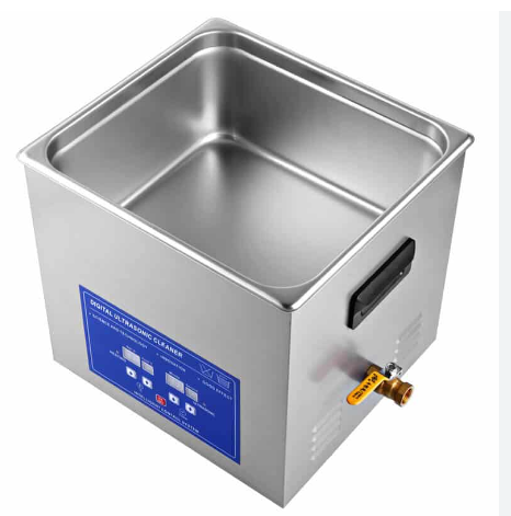
Following the preparation and solution selection, the ultrasonic cleaner must be set up.
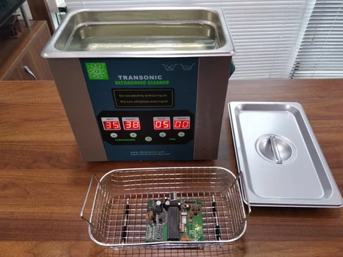
This involves filling the cleaner’s tank with the chosen solution and ensuring that the solution level is sufficient to fully submerge the PCBs. It is also important to set the correct temperature, as most cleaning solutions perform optimally at elevated temperatures, usually between 50°C and 60°C. Once the tank is filled and the temperature is set, the ultrasonic cleaner should be turned on to allow the solution to degas. Degassing is the process of removing dissolved gases from the solution, which can interfere with the cavitation process. This typically takes about 10 to 15 minutes.
With the ultrasonic cleaner ready, the PCBs can now be placed into the cleaning tank.
It is advisable to use a basket or a holder to keep the PCBs suspended in the solution, ensuring even exposure to the ultrasonic waves. The cleaning duration depends on the level of contamination and the complexity of the PCB design but generally ranges from 3 to 10 minutes. During this time, the ultrasonic waves generate cavitation bubbles that effectively clean the PCBs by reaching into tiny crevices and under components where manual cleaning cannot.
After the cleaning cycle is complete, the PCBs must be thoroughly rinsed to remove any residual cleaning solution.
This is typically done using deionized water to prevent any mineral deposits from forming on the PCB surfaces. The rinsing process should be thorough to ensure that all traces of the cleaning solution are removed, as any residue left behind can potentially cause corrosion or electrical issues.
The final step in the ultrasonic PCB cleaning process is drying the PCBs.
Proper drying is crucial to prevent moisture-related damage. This can be achieved using a combination of air drying, forced air, or specialized drying equipment such as a drying oven. It is important to ensure that the PCBs are completely dry before they are reassembled or put back into service.
In conclusion, ultrasonic PCB cleaning is a meticulous yet highly effective method for ensuring that PCBs are free from contaminants. By following a structured approach that includes preparation, solution selection, ultrasonic cleaning, rinsing, and drying, one can achieve optimal cleaning results, thereby enhancing the performance and longevity of the PCBs.
Comparing Ultrasonic Cleaning To Traditional PCB Cleaning Methods
Ultrasonic PCB cleaning has emerged as a sophisticated method for ensuring the cleanliness and functionality of printed circuit boards (PCBs). When comparing ultrasonic cleaning to traditional PCB cleaning methods, it is essential to consider various factors such as efficiency, effectiveness, environmental impact, and cost. Traditional methods, such as manual scrubbing, brushing, and solvent cleaning, have been widely used for decades. However, these methods often fall short in several critical areas, particularly when dealing with intricate and densely populated PCBs.
One of the primary advantages of ultrasonic cleaning over traditional methods is its superior ability to reach and clean complex geometries and hard-to-reach areas.
Ultrasonic cleaning employs high-frequency sound waves to create microscopic cavitation bubbles in a cleaning solution. These bubbles implode upon contact with the PCB surface, effectively dislodging contaminants such as flux residues, solder paste, and other particulate matter. In contrast, manual scrubbing and brushing can be labor-intensive and may not adequately clean areas beneath components or within tight spaces, leading to potential reliability issues.
Moreover, ultrasonic cleaning is known for its consistency and repeatability.
Traditional methods often rely on the skill and diligence of the operator, which can result in variability in the cleaning process. In contrast, ultrasonic cleaning systems can be precisely controlled and programmed to deliver consistent results, ensuring that each PCB is cleaned to the same high standard. This level of consistency is particularly crucial in industries where reliability and performance are paramount, such as aerospace, medical devices, and telecommunications.
Another significant consideration is the environmental impact of the cleaning process.
Traditional solvent-based cleaning methods can involve the use of hazardous chemicals that pose risks to both human health and the environment. These solvents often require special handling, disposal procedures, and can contribute to volatile organic compound (VOC) emissions. Ultrasonic cleaning, on the other hand, typically uses water-based solutions that are less harmful and easier to manage. This shift towards more environmentally friendly cleaning solutions aligns with the growing emphasis on sustainability and regulatory compliance in the electronics manufacturing industry.
Cost is another factor where ultrasonic cleaning can offer advantages.
While the initial investment in ultrasonic cleaning equipment may be higher than that for traditional methods, the long-term benefits often outweigh the upfront costs. Ultrasonic cleaning systems can reduce labor costs by automating the cleaning process and minimizing the need for manual intervention. Additionally, the extended lifespan and improved reliability of PCBs cleaned ultrasonically can lead to lower failure rates and reduced warranty claims, ultimately resulting in cost savings for manufacturers.
Furthermore, ultrasonic cleaning can enhance the overall quality and performance of PCBs.
By thoroughly removing contaminants, ultrasonic cleaning helps prevent issues such as electrical shorts, corrosion, and signal interference, which can compromise the functionality of electronic devices. This level of cleanliness is particularly important in high-reliability applications where even minor contaminants can lead to significant failures.
In conclusion, while traditional PCB cleaning methods have their place, ultrasonic cleaning offers numerous advantages that make it a superior choice for many applications. Its ability to clean complex geometries, deliver consistent results, reduce environmental impact, and provide long-term cost savings makes it an attractive option for modern electronics manufacturing. As technology continues to advance and the demand for high-quality, reliable electronic devices grows, the adoption of ultrasonic PCB cleaning is likely to become increasingly prevalent.