Techniques for high speed adc pcb layout
Optimizing Signal Integrity in High Speed ADC PCB Layout
Optimizing signal integrity in high-speed ADC PCB layout is a critical aspect of modern electronic design, as it directly impacts the performance and reliability of the system. To achieve optimal signal integrity, several techniques must be employed, each addressing different aspects of the layout process.
One of the primary considerations is the careful management of trace impedance.
Ensuring that the impedance of signal traces is consistent and matches the characteristic impedance of the ADC inputs is essential. This can be achieved by controlling the trace width, spacing, and the dielectric properties of the PCB material. Additionally, the use of differential signaling can significantly enhance signal integrity by reducing susceptibility to electromagnetic interference (EMI) and crosstalk.
Another crucial technique involves the strategic placement of components.
Placing the ADC as close as possible to the signal source minimizes the length of the signal path, thereby reducing the potential for signal degradation. Furthermore, it is important to place decoupling capacitors near the power pins of the ADC to filter out noise and provide a stable power supply. The use of ground planes is also vital in maintaining signal integrity. A continuous ground plane beneath the signal traces provides a low-impedance return path for the signals, which helps to minimize noise and EMI.
In addition to component placement, the routing of signal traces plays a significant role in optimizing signal integrity.
High-speed signal traces should be routed with minimal bends and should avoid sharp angles, as these can cause signal reflections and impedance discontinuities. When routing differential pairs, it is essential to maintain equal trace lengths and consistent spacing to ensure that the signals remain synchronized. Moreover, it is advisable to route high-speed signals on internal layers of the PCB, sandwiched between ground planes, to shield them from external noise sources.
The use of vias should be minimized in high-speed ADC PCB layouts, as they can introduce inductance and capacitance that degrade signal quality.
When vias are necessary, it is important to use them sparingly and to ensure that they are properly back-drilled to remove any unused stubs. Additionally, the use of controlled impedance vias can help to maintain signal integrity by providing a consistent impedance path through the PCB.
Power integrity is another critical aspect of high-speed ADC PCB layout.
Ensuring a clean and stable power supply to the ADC is essential for optimal performance. This can be achieved by using low-impedance power planes and by implementing proper decoupling techniques. The use of multiple decoupling capacitors with different values can help to filter out a wide range of noise frequencies. Furthermore, the placement of power and ground vias should be carefully considered to minimize the loop area and reduce the potential for noise coupling.
Thermal management is also an important consideration in high-speed ADC PCB layout.
High-speed ADCs can generate significant amounts of heat, which can affect their performance and reliability. Proper thermal management techniques, such as the use of thermal vias and heat sinks, can help to dissipate heat and maintain the ADC within its optimal operating temperature range.
In conclusion, optimizing signal integrity in high-speed ADC PCB layout requires a comprehensive approach that addresses trace impedance, component placement, signal routing, via management, power integrity, and thermal management. By carefully considering each of these factors and employing the appropriate techniques, designers can ensure that their high-speed ADCs perform reliably and efficiently in their intended applications.
Effective Grounding Strategies for High-Speed ADCs
Effective grounding strategies are paramount when designing printed circuit boards (PCBs) for high-speed analog-to-digital converters (ADCs). Proper grounding ensures signal integrity, minimizes noise, and enhances overall system performance.
One fundamental principle is to establish a solid ground plane.
A continuous, unbroken ground plane provides a low-impedance path for return currents, reducing the potential for noise and electromagnetic interference (EMI). This approach also helps in maintaining a consistent reference voltage across the PCB, which is crucial for the accurate operation of high-speed ADCs.
In addition to a solid ground plane, it is essential to consider the placement of components and routing of traces.
Placing the ADC and its associated components, such as reference voltage sources and decoupling capacitors, close to each other minimizes the length of signal paths. Shorter paths reduce inductance and resistance, which in turn decreases the likelihood of noise coupling into the signal. Furthermore, routing high-speed signals over the ground plane ensures that the return currents follow the path of least impedance, thereby reducing loop areas and minimizing EMI.
Another effective grounding strategy involves the use of multiple ground planes.
In multilayer PCBs, dedicating separate layers for analog and digital grounds can significantly reduce noise coupling between the two domains. However, it is crucial to connect these ground planes at a single point, often referred to as a star ground or single-point ground. This connection point should be strategically placed near the ADC to ensure that any potential differences between the analog and digital grounds do not affect the ADC’s performance.
Decoupling capacitors play a vital role in effective grounding strategies.
Placing these capacitors close to the power pins of the ADC and other critical components helps filter out high-frequency noise. The choice of capacitor values is also important; a combination of capacitors with different values, such as 0.1 µF and 10 µF, can provide effective filtering across a wide frequency range. Additionally, using low-ESR (Equivalent Series Resistance) capacitors can further enhance noise suppression.
Grounding strategies must also account for the layout of power and ground traces.
Ensuring that power and ground traces are wide and short reduces their impedance, which is particularly important for high-speed ADCs that require stable and clean power supplies. Moreover, using a ground pour or copper pour technique can enhance the grounding by increasing the surface area of the ground plane, thereby reducing impedance and improving thermal performance.
Shielding is another technique that can be employed to enhance grounding effectiveness.
Placing a grounded shield around sensitive analog components and traces can protect them from external noise sources. This is particularly useful in environments with high levels of EMI. The shield should be connected to the ground plane at multiple points to ensure effective noise suppression.
In conclusion, effective grounding strategies are critical for the optimal performance of high-speed ADCs in PCB layouts. By implementing a solid ground plane, carefully placing components, using multiple ground planes with a single-point connection, employing decoupling capacitors, optimizing power and ground trace layouts, and incorporating shielding, designers can significantly enhance signal integrity and reduce noise. These strategies collectively contribute to the reliable and accurate operation of high-speed ADCs, ensuring that they meet the stringent performance requirements of modern electronic systems.
Minimizing Crosstalk in High-Speed ADC PCB Designs
Minimizing crosstalk in high-speed ADC PCB designs is a critical aspect of ensuring signal integrity and overall system performance. Crosstalk, which refers to the unwanted coupling of signals between adjacent traces, can significantly degrade the performance of high-speed analog-to-digital converters (ADCs). Therefore, implementing effective techniques to mitigate crosstalk is essential for achieving accurate and reliable data conversion.
One of the primary strategies for minimizing crosstalk is to maintain adequate spacing between signal traces.
By increasing the distance between adjacent traces, the potential for electromagnetic interference (EMI) is reduced. This can be achieved by adhering to the design rules specified by the PCB manufacturer, which typically recommend a minimum spacing based on the operating frequency and signal characteristics. Additionally, employing differential signaling can further reduce crosstalk, as it involves using pairs of traces that carry equal and opposite signals, thereby canceling out any induced noise.
Another effective technique is to use ground planes and power planes strategically.
Ground planes act as a reference point for signals and provide a low-impedance path for return currents, which helps to minimize the loop area and, consequently, the potential for crosstalk. Placing a continuous ground plane beneath the signal layers can significantly reduce the coupling between traces. Moreover, ensuring that the ground plane is uninterrupted and free of splits or gaps is crucial, as discontinuities can lead to increased EMI and crosstalk.
In addition to ground planes, the use of guard traces can be beneficial.
Guard traces are grounded traces placed between high-speed signal lines to provide additional shielding and isolation. These traces can absorb and dissipate any coupled noise, thereby reducing the impact of crosstalk on the signal integrity. It is important to connect the guard traces to the ground plane at regular intervals to maintain their effectiveness.
Furthermore, careful routing of signal traces is essential in minimizing crosstalk.
Avoiding parallel routing of high-speed signals over long distances can significantly reduce the potential for interference. Instead, routing traces at right angles or using serpentine routing can help to minimize the coupling between adjacent traces. Additionally, keeping high-speed signal traces away from noisy components, such as power supplies and switching regulators, can further reduce the risk of crosstalk.
The use of proper termination techniques is also crucial in mitigating crosstalk.
Termination resistors can be placed at the end of signal traces to match the impedance of the transmission line, thereby reducing reflections and minimizing the potential for crosstalk. Both series and parallel termination methods can be employed, depending on the specific requirements of the design.
Moreover, employing advanced PCB materials with low dielectric constants and low loss tangents can help to reduce crosstalk.
These materials exhibit lower levels of signal attenuation and dispersion, which can improve signal integrity and reduce the potential for interference. Selecting the appropriate PCB material based on the operating frequency and signal characteristics is essential for optimizing the performance of high-speed ADC designs.
In conclusion, minimizing crosstalk in high-speed ADC PCB designs requires a comprehensive approach that includes maintaining adequate spacing between traces, using ground and power planes effectively, employing guard traces, careful routing of signal traces, proper termination techniques, and selecting advanced PCB materials. By implementing these techniques, designers can significantly enhance signal integrity and ensure the reliable operation of high-speed ADCs in various applications.
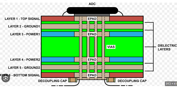
Power Supply Decoupling Techniques for High-Speed ADCs
In the realm of high-speed Analog-to-Digital Converters (ADCs), power supply decoupling is a critical aspect that can significantly influence the performance and accuracy of the system. Proper decoupling techniques are essential to mitigate noise and ensure stable operation. To achieve optimal results, it is imperative to understand and implement effective power supply decoupling strategies.
Firstly, the selection of decoupling capacitors is paramount.
Capacitors with low Equivalent Series Resistance (ESR) and low Equivalent Series Inductance (ESL) are preferred, as they can effectively filter out high-frequency noise. Ceramic capacitors, particularly those with X7R or C0G/NP0 dielectric materials, are commonly used due to their stability and low loss characteristics. It is advisable to use a combination of capacitors with different values, such as 0.1 µF, 1 µF, and 10 µF, to cover a broad range of frequencies. This multi-capacitor approach ensures that both high-frequency and low-frequency noise components are adequately suppressed.
In addition to selecting appropriate capacitors, their placement on the PCB is equally crucial.
Decoupling capacitors should be placed as close as possible to the power pins of the ADC. This minimizes the inductive effects of the PCB traces, which can otherwise degrade the capacitor’s effectiveness. Furthermore, placing the capacitors on the same layer as the ADC, rather than on the opposite side of the board, reduces the loop area and associated inductance, thereby enhancing the decoupling performance.
Another important consideration is the use of a solid ground plane.
A continuous ground plane provides a low-impedance return path for the decoupling currents, which is essential for maintaining signal integrity. It also helps to reduce electromagnetic interference (EMI) by providing effective shielding. When designing the PCB, it is beneficial to allocate a dedicated layer for the ground plane, ensuring that it is as unbroken as possible. Any splits or gaps in the ground plane can create potential differences and increase noise susceptibility.
Moreover, the power supply routing should be carefully planned.
Power traces should be kept short and wide to minimize resistance and inductance. It is also advantageous to use multiple vias to connect the decoupling capacitors to the power and ground planes, as this reduces the inductive impedance and improves the overall decoupling efficiency. Additionally, employing a star routing topology, where each power supply branch radiates from a central point, can help to isolate noise sources and prevent cross-coupling between different sections of the circuit.
To further enhance power supply decoupling, the use of ferrite beads can be considered.
Ferrite beads act as high-frequency filters, attenuating noise above a certain threshold while allowing DC and low-frequency signals to pass through. Placing ferrite beads in series with the power supply lines can effectively block high-frequency noise from reaching the ADC. However, it is important to select ferrite beads with appropriate current ratings and impedance characteristics to avoid unwanted signal attenuation.
In conclusion, effective power supply decoupling for high-speed ADCs involves a combination of selecting suitable capacitors, strategic placement, maintaining a solid ground plane, careful power routing, and potentially incorporating ferrite beads. By meticulously implementing these techniques, one can significantly enhance the performance and reliability of high-speed ADC systems, ensuring accurate and stable operation in demanding applications.