Steps involved in pcb manufacturing
Steps involved in pcb manufacturing
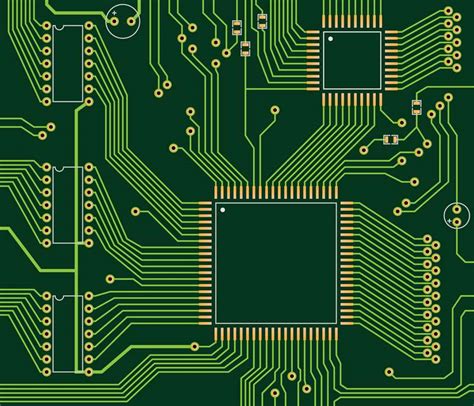
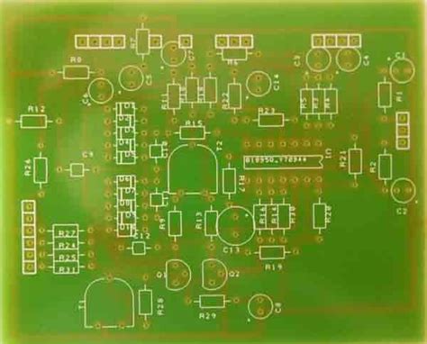
Designing the PCB layout is a critical phase in the manufacturing process of printed circuit boards (PCBs). This stage involves translating the schematic diagram into a physical representation that can be fabricated.
The process begins with the creation of a schematic, which is essentially a blueprint of the electronic circuit. This schematic is developed using specialized software tools that allow engineers to place and connect various electronic components such as resistors, capacitors, and integrated circuits.
Once the schematic is complete, the next step is to define the board outline.
This involves specifying the dimensions and shape of the PCB, which can vary depending on the application. The board outline serves as a boundary within which all components and traces must fit. Following this, the placement of components is carried out. This step is crucial as it affects the performance, manufacturability, and reliability of the PCB. Components are strategically placed to minimize signal interference, reduce trace lengths, and ensure thermal management.
After the components are placed, the routing process begins.
Routing involves creating electrical connections between the components using copper traces. This step is highly intricate and requires careful consideration of various factors such as signal integrity, impedance control, and electromagnetic compatibility. Engineers use design rules and constraints to guide the routing process, ensuring that the traces do not overlap and that they maintain adequate spacing to prevent short circuits.
In addition to routing, the design of power and ground planes is also essential.
These planes provide a stable reference voltage and help in reducing noise and electromagnetic interference. The power and ground planes are typically placed on separate layers of the PCB, and their design must ensure that they can handle the required current without causing voltage drops or overheating.
Once the routing and plane design are complete, the next step is to perform a design rule check (DRC).
The DRC is an automated process that verifies the PCB layout against a set of predefined rules. These rules include minimum trace width, spacing between traces, and clearance from the board edge. The DRC helps in identifying potential issues that could affect the manufacturability or performance of the PCB.
Following the DRC, a signal integrity analysis is conducted.
This analysis evaluates the quality of the electrical signals as they travel through the traces. It helps in identifying issues such as signal reflection, crosstalk, and timing delays, which can affect the performance of high-speed circuits. Based on the results of the signal integrity analysis, adjustments may be made to the layout to optimize signal quality.
The final step in designing the PCB layout is to generate the fabrication files.
These files include Gerber files, drill files, and a bill of materials (BOM). Gerber files contain the information needed to create the copper layers, solder mask, and silkscreen. Drill files specify the locations and sizes of holes to be drilled in the PCB. The BOM lists all the components required for assembly, along with their specifications.
In conclusion, designing the PCB layout is a meticulous process that involves several steps, each critical to the successful fabrication and performance of the final product. From creating the schematic to generating the fabrication files, each phase requires careful planning and attention to detail. By following these steps, engineers can ensure that the PCB meets the desired specifications and functions reliably in its intended application.
Creating The Photomask
Creating the photomask is a critical step in the manufacturing of printed circuit boards (PCBs), serving as the blueprint for the intricate patterns of conductive pathways that will be etched onto the board.
This process begins with the design phase, where engineers use specialized software to create a detailed layout of the circuit.
The design is meticulously checked for errors, ensuring that all connections are accurate and that the layout adheres to the specified electrical and mechanical constraints. Once the design is finalized, it is converted into a format suitable for photomask creation, typically a Gerber file.
The next step involves transferring the digital design onto a physical medium.
This is achieved by using a photoplotter, a high-precision device that translates the digital data into a photomask. The photoplotter uses a laser or a light-emitting diode (LED) to expose the design onto a photosensitive film or glass plate.
The choice of material for the photomask depends on the required resolution and the specific needs of the PCB being manufactured. For high-precision applications, glass plates are preferred due to their stability and ability to hold fine details.
After the exposure process, the photomask undergoes a development phase.
This involves immersing the exposed film or glass plate in a chemical developer that reveals the latent image created by the photoplotter. The development process must be carefully controlled to ensure that the image is sharp and free of defects. Any imperfections at this stage can lead to errors in the final PCB, making quality control a critical aspect of photomask creation.
Following development, the photomask is subjected to a series of inspections to verify its accuracy.
Automated optical inspection (AOI) systems are commonly used to compare the photomask against the original design file. These systems can detect even the smallest deviations, ensuring that the photomask is an exact replica of the intended design. In addition to AOI, manual inspections are often conducted to catch any anomalies that automated systems might miss. This dual-layered approach to quality control helps to guarantee the reliability of the photomask.
Once the photomask has passed all inspections, it is ready for use in the PCB manufacturing process.
The photomask is placed over a copper-clad laminate, which has been coated with a layer of photoresist. The assembly is then exposed to ultraviolet (UV) light, which hardens the photoresist in the areas exposed through the transparent sections of the photomask. The unexposed areas of the photoresist remain soft and can be washed away, leaving behind a precise pattern of hardened photoresist that mirrors the design on the photomask.
This pattern serves as a protective barrier during the etching process, where a chemical solution removes the unprotected copper, leaving behind the desired circuit pathways. The accuracy of the photomask directly influences the precision of the etched circuit, making it a cornerstone of PCB manufacturing.
In conclusion, creating the photomask is a meticulous process that involves several stages, from design and exposure to development and inspection. Each step is crucial in ensuring that the final PCB meets the required specifications and functions as intended. The photomask serves as the foundation upon which the entire PCB is built, highlighting its importance in the overall manufacturing process.
Etching The PCB
Etching the PCB is a critical step in the manufacturing process, transforming a blank copper-clad board into a functional printed circuit board (PCB) with intricate pathways for electrical signals. This process involves several meticulous stages, each contributing to the precise removal of unwanted copper to reveal the desired circuit pattern. Understanding these steps is essential for appreciating the complexity and precision required in PCB manufacturing.
Initially, the PCB starts as a flat, copper-coated substrate.
The first step in the etching process is to apply a protective layer, known as a resist, over the areas of the copper that need to remain intact. This resist can be applied using various methods, such as screen printing, photoresist application, or dry film lamination. Photoresist is particularly common due to its precision and ease of use. It involves coating the board with a light-sensitive material that hardens when exposed to ultraviolet (UV) light.
Once the resist is applied, the board undergoes a process called photolithography.
During this stage, a photomask, which contains the desired circuit pattern, is placed over the board. The board is then exposed to UV light, which hardens the photoresist in the areas not covered by the photomask. The unexposed areas of the photoresist remain soft and can be washed away using a developer solution, revealing the underlying copper that needs to be etched away.
Following the development stage, the board is ready for the actual etching process.
The most common etching method involves using a chemical solution, typically ferric chloride or ammonium persulfate, to dissolve the exposed copper. The board is immersed in the etching solution, and the chemical reaction selectively removes the unwanted copper, leaving behind the protected areas covered by the hardened resist. This step requires careful control of the etching time and solution concentration to ensure precise removal of copper without damaging the desired circuit pattern.
After etching, the board is thoroughly cleaned to remove any residual etching solution and resist material.
This cleaning process is crucial to prevent any contamination that could affect the board’s performance. The resist is usually stripped away using a solvent or a specialized stripping solution, revealing the final copper traces that form the circuit.
To ensure the quality and accuracy of the etched PCB, it undergoes a series of inspections.
Visual inspection is the first step, where technicians check for any obvious defects or irregularities in the copper traces. Automated optical inspection (AOI) systems are also employed to compare the etched board against the original design files, identifying any discrepancies that may have occurred during the etching process.
In conclusion, etching the PCB is a complex and precise process that involves several critical steps, from applying the resist and photolithography to chemical etching and thorough cleaning. Each stage requires careful attention to detail and precise control to ensure the final PCB meets the required specifications and functions correctly. Understanding these steps highlights the intricate nature of PCB manufacturing and the importance of precision in creating reliable and high-quality electronic components.
Assembling And Testing The PCB
Assembling and testing a printed circuit board (PCB) is a meticulous process that demands precision and attention to detail. The assembly phase begins with the placement of components onto the PCB. This step is typically executed using surface-mount technology (SMT), where components are mounted directly onto the surface of the board. Automated machines, known as pick-and-place machines, are employed to position these components accurately. These machines are programmed to place each component in its designated location, ensuring that the assembly process is both efficient and precise.
Following the placement of components, the next step involves soldering.
Soldering is crucial as it secures the components to the PCB and establishes electrical connections. There are two primary methods of soldering: reflow soldering and wave soldering. Reflow soldering is commonly used for SMT components. In this method, the PCB, with components placed on it, is passed through a reflow oven. The oven heats the board to a temperature that melts the solder paste, creating a strong bond between the components and the PCB. On the other hand, wave soldering is typically used for through-hole components. In this process, the PCB is passed over a wave of molten solder, which adheres to the exposed metal areas, forming the necessary connections.
Once soldering is complete, the PCB undergoes a thorough inspection to ensure that all components are correctly placed and soldered.
This inspection can be performed using automated optical inspection (AOI) systems, which use cameras to capture images of the PCB and compare them to a predefined standard. Any discrepancies, such as misplaced components or soldering defects, are flagged for correction. Additionally, X-ray inspection may be employed to examine solder joints that are not visible to the naked eye, particularly in the case of complex or densely populated PCBs.
After the inspection phase, the PCB is subjected to electrical testing to verify its functionality.
One common method of testing is the in-circuit test (ICT), which checks for shorts, opens, resistance, capacitance, and other basic parameters. ICT involves using a bed of nails tester, which makes contact with various points on the PCB to perform these checks. Another method is the functional test, which evaluates the PCB’s performance under real-world conditions. This test involves applying power to the PCB and running it through a series of operations to ensure it functions as intended.
In addition to these tests, some PCBs may require burn-in testing, where the board is operated at elevated temperatures and voltages for an extended period.
This process helps identify any potential early-life failures and ensures the long-term reliability of the PCB. Once all testing is complete and the PCB has passed all quality checks, it is ready for final assembly into the end product.
Throughout the entire assembly and testing process, maintaining a clean and controlled environment is essential. Contaminants such as dust and moisture can adversely affect the performance and reliability of the PCB. Therefore, assembly facilities often employ cleanroom standards and use anti-static measures to protect sensitive electronic components.
In conclusion, assembling and testing a PCB involves a series of precise and carefully monitored steps, from component placement and soldering to inspection and electrical testing. Each phase is critical to ensuring the final product meets the required specifications and performs reliably in its intended application.