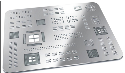
Stencil for pcb assembly
Benefits Of Using Stencil for PCB Assembly
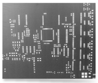
In the realm of printed circuit board (PCB) assembly, the utilization of stencils has become an indispensable practice, offering a multitude of benefits that significantly enhance the efficiency and quality of the manufacturing process. Stencils, typically made from stainless steel or other durable materials, serve as precise templates for the application of solder paste onto the PCB. This method ensures that the solder paste is deposited accurately onto the designated pads, which is crucial for the subsequent placement and soldering of electronic components.
One of the primary advantages of using stencils in PCB assembly is the remarkable improvement in accuracy and consistency.
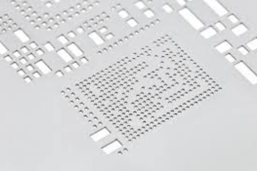
Manual application of solder paste can lead to variations in the amount and placement of the paste, which can result in defects such as solder bridges, insufficient solder joints, or misaligned components. Stencils, however, are designed with exact apertures that correspond to the layout of the PCB, ensuring that the right amount of solder paste is applied uniformly across all pads. This precision is particularly vital for high-density PCBs, where the components are closely packed, and even minor deviations can cause significant issues.
Moreover, the use of stencils in PCB assembly contributes to a substantial increase in production speed.
In a manual process, applying solder paste to each pad individually is time-consuming and labor-intensive. Stencils streamline this step by allowing the simultaneous application of solder paste to all pads in a single pass. This efficiency not only accelerates the assembly process but also reduces labor costs, making it a cost-effective solution for both small-scale and large-scale production runs.
In addition to enhancing accuracy and speed, stencils also play a crucial role in improving the overall reliability and performance of the final product.
Consistent and precise application of solder paste ensures robust solder joints, which are essential for the electrical and mechanical integrity of the PCB. Reliable solder joints minimize the risk of component failure, thereby enhancing the durability and longevity of the electronic device. This reliability is particularly critical in applications where the PCB is subjected to harsh operating conditions or where failure could have severe consequences, such as in medical devices, aerospace, and automotive electronics.
Furthermore, the use of stencils in PCB assembly facilitates better process control and quality assurance.
By standardizing the solder paste application process, stencils help in maintaining uniformity across multiple production batches. This standardization simplifies the inspection and testing procedures, as the likelihood of defects caused by inconsistent solder paste application is significantly reduced. Consequently, manufacturers can achieve higher yields and lower the incidence of rework or scrap, leading to more efficient and cost-effective production.
Another noteworthy benefit of using stencils is their adaptability to various PCB designs and manufacturing requirements.
Stencils can be customized to accommodate different pad sizes, shapes, and configurations, making them suitable for a wide range of PCB applications. This flexibility allows manufacturers to easily adapt to design changes or new product developments without compromising on the quality or efficiency of the assembly process.
In conclusion, the integration of stencils in PCB assembly offers numerous advantages that collectively enhance the precision, speed, reliability, and cost-effectiveness of the manufacturing process. By ensuring accurate and consistent application of solder paste, stencils play a pivotal role in producing high-quality PCBs that meet stringent performance and reliability standards. As the demand for sophisticated electronic devices continues to grow, the importance of stencils in achieving efficient and reliable PCB assembly cannot be overstated.
How To Choose The Right Stencil For Your PCB Design
Choosing the right stencil for your PCB design is a critical step in ensuring the success of your printed circuit board assembly. The stencil plays a pivotal role in the solder paste application process, which directly impacts the quality and reliability of the final product. Therefore, understanding the various factors that influence stencil selection is essential for achieving optimal results.
To begin with, the type of stencil material is a primary consideration.
Stencils are typically made from stainless steel or nickel, each offering distinct advantages. Stainless steel stencils are known for their durability and precision, making them suitable for high-volume production runs. On the other hand, nickel stencils provide superior flexibility and are often preferred for complex designs with fine-pitch components. Consequently, the choice between stainless steel and nickel should be guided by the specific requirements of your PCB design and production volume.
Another crucial factor is the thickness of the stencil.
The thickness determines the amount of solder paste deposited on the PCB pads, which in turn affects the solder joint quality. Thicker stencils deposit more solder paste, which is beneficial for larger components but may lead to bridging issues in fine-pitch areas. Conversely, thinner stencils provide better control for fine-pitch components but may result in insufficient solder for larger pads. Therefore, selecting the appropriate stencil thickness requires a careful balance based on the component sizes and pad geometries in your design.
In addition to material and thickness, the aperture design of the stencil is equally important.
The apertures must be precisely aligned with the PCB pads to ensure accurate solder paste deposition. Laser-cut stencils offer high precision and are ideal for intricate designs with tight tolerances. Moreover, the shape and size of the apertures can be optimized to enhance solder paste release and minimize defects. For instance, rounded corners on rectangular apertures can improve paste release and reduce the risk of clogging. Thus, meticulous attention to aperture design can significantly enhance the performance of the stencil.
Furthermore, the type of surface finish on the stencil can influence its effectiveness.
Electropolished stencils have a smoother surface, which facilitates better solder paste release and reduces the likelihood of defects. This finish is particularly beneficial for fine-pitch components and high-density designs. While electropolished stencils may come at a higher cost, the improvement in yield and reliability often justifies the investment. Therefore, considering the surface finish is an important aspect of stencil selection.
Additionally, the method of stencil alignment during the assembly process should not be overlooked.
Proper alignment ensures that the solder paste is accurately deposited on the PCB pads, which is crucial for achieving reliable solder joints. Automated stencil printers with vision systems offer precise alignment and are recommended for high-precision applications. Manual alignment, while cost-effective, may introduce variability and is generally suitable for low-volume or prototype runs. Hence, the alignment method should be chosen based on the complexity and volume of your PCB assembly.
In conclusion, selecting the right stencil for your PCB design involves a comprehensive evaluation of various factors, including material, thickness, aperture design, surface finish, and alignment method. By carefully considering these aspects, you can ensure accurate solder paste deposition, which is fundamental to the quality and reliability of your PCB assembly. As such, investing time and effort in choosing the appropriate stencil can lead to significant improvements in the overall performance and success of your electronic products.
Step-By-Step Guide To Creating A Custom PCB Stencil
Creating a custom PCB stencil is a meticulous process that requires precision and attention to detail. This guide will walk you through the essential steps to ensure that your stencil is both accurate and effective for PCB assembly.
The first step in creating a custom PCB stencil is to design your PCB layout using specialized software.
Programs such as Eagle, KiCad, or Altium Designer are commonly used for this purpose. These tools allow you to create a detailed schematic of your circuit, which will serve as the blueprint for your stencil. Once your design is complete, you will need to export the Gerber files, which contain the necessary information for stencil creation.
After obtaining the Gerber files, the next step is to select the appropriate material for your stencil.
Stainless steel and polyimide are popular choices due to their durability and precision. Stainless steel stencils are particularly favored for their longevity and ability to produce fine-pitch components. Polyimide stencils, on the other hand, are more flexible and can be a cost-effective alternative for smaller production runs. With the material chosen, you will then need to decide on the thickness of the stencil. The thickness will depend on the type of components you are using and the amount of solder paste required. Typically, a thickness of 0.1mm to 0.2mm is suitable for most applications.
Following the material selection, the next phase involves the actual cutting of the stencil.
Laser cutting is the preferred method due to its high precision and ability to create clean, accurate apertures. The Gerber files are loaded into the laser cutting machine, which then meticulously cuts out the stencil according to the design specifications. It is crucial to ensure that the apertures are cut accurately to avoid any issues during the solder paste application process. Any deviations can lead to solder bridging or insufficient solder deposits, which can compromise the integrity of the PCB assembly.
Once the stencil has been cut, it is essential to inspect it thoroughly for any defects or irregularities.
This step is critical to ensure that the stencil will perform as expected during the solder paste application. Use a magnifying glass or microscope to examine the apertures and edges for any signs of burrs or misalignment. If any defects are found, they should be addressed immediately to prevent any issues during the assembly process.
The final step in creating a custom PCB stencil is to mount it onto a frame.
The frame provides stability and ensures that the stencil remains flat during the solder paste application. There are various types of frames available, including fixed and adjustable frames. Fixed frames are more rigid and provide better stability, while adjustable frames offer more flexibility and can be used with different stencil sizes. Once the stencil is mounted, it is ready for use in the PCB assembly process.
In conclusion, creating a custom PCB stencil involves several critical steps, from designing the PCB layout and selecting the appropriate material to cutting the stencil and inspecting it for defects. Each step requires careful attention to detail to ensure that the final stencil is accurate and effective. By following this step-by-step guide, you can create a custom PCB stencil that will facilitate a smooth and efficient assembly process, ultimately leading to high-quality PCB production.
Common Mistakes To Avoid When Using PCB Stencils
When using stencils for PCB assembly, it is crucial to be aware of common mistakes that can compromise the quality and functionality of the final product. One frequent error is the improper alignment of the stencil with the PCB. Misalignment can lead to solder paste being applied inaccurately, which in turn can cause bridging, insufficient solder joints, or open circuits. To avoid this, it is essential to use alignment tools and techniques, such as fiducial markers, to ensure precise positioning of the stencil over the PCB.
Another common mistake is the use of an inappropriate stencil thickness.
The thickness of the stencil directly affects the volume of solder paste deposited on the PCB pads. If the stencil is too thick, it can result in excessive solder paste, leading to solder bridging and short circuits. Conversely, a stencil that is too thin may not deposit enough solder paste, causing weak or incomplete solder joints. Therefore, selecting the correct stencil thickness based on the specific requirements of the PCB design is vital for achieving optimal results.
In addition to alignment and thickness issues, the cleanliness of the stencil is another critical factor that can impact the quality of the PCB assembly.
Residual solder paste or contaminants on the stencil can cause defects in the solder paste deposition process. Regular cleaning of the stencil, using appropriate cleaning agents and methods, is necessary to maintain its effectiveness and ensure consistent solder paste application. Neglecting this aspect can lead to repeated defects and increased rework, ultimately affecting the overall efficiency of the assembly process.
Furthermore, the type of solder paste used in conjunction with the stencil plays a significant role in the success of the PCB assembly.
Using solder paste that is not compatible with the stencil material or the specific application can result in poor adhesion, inconsistent deposition, and other issues. It is important to select solder paste that matches the stencil’s material properties and the requirements of the PCB design. Additionally, proper storage and handling of solder paste are essential to maintain its quality and performance.
Another mistake to avoid is the improper handling and storage of the stencil itself.
Stencils are delicate and can be easily damaged if not handled with care. Bending, scratching, or denting the stencil can lead to inaccuracies in solder paste deposition. Stencils should be stored in a clean, dry environment and handled using appropriate tools and techniques to prevent damage. Regular inspection of the stencil for any signs of wear or damage is also recommended to ensure its continued effectiveness.
Moreover, the squeegee pressure and speed during the solder paste application process are critical parameters that need to be carefully controlled.
Excessive pressure or speed can cause the stencil to flex or shift, leading to uneven solder paste deposition. On the other hand, insufficient pressure or speed may result in incomplete filling of the stencil apertures. It is important to optimize these parameters based on the specific characteristics of the stencil and the solder paste to achieve consistent and accurate results.
Lastly, neglecting to perform regular maintenance and calibration of the stencil printing equipment can lead to a decline in performance over time.
Equipment that is not properly maintained or calibrated can cause misalignment, inconsistent pressure, and other issues that affect the quality of the solder paste deposition. Implementing a routine maintenance schedule and ensuring that the equipment is regularly calibrated can help prevent these problems and ensure the reliability of the PCB assembly process.
In conclusion, avoiding common mistakes when using PCB stencils requires careful attention to alignment, stencil thickness, cleanliness, solder paste compatibility, handling and storage, squeegee pressure and speed, and equipment maintenance. By addressing these factors, manufacturers can achieve higher quality and more reliable PCB assemblies, ultimately leading to better performance and customer satisfaction.