Stack up flex pcb
Advantages Of Using Stack Up Flex PCB In Modern Electronics
The integration of stack up flex PCBs in modern electronics has revolutionized the way devices are designed and manufactured, offering a multitude of advantages that cater to the evolving demands of the industry.
One of the primary benefits of stack up flex PCBs is their remarkable flexibility, which allows for the creation of complex, three-dimensional circuit designs.
This flexibility is particularly advantageous in applications where space constraints are a significant concern, such as in wearable technology, medical devices, and compact consumer electronics. By enabling circuits to bend and fold, stack up flex PCBs facilitate the development of smaller, lighter, and more efficient devices.
In addition to their physical flexibility, stack up flex PCBs also offer enhanced reliability and durability.
Traditional rigid PCBs are prone to mechanical stress and potential failure when subjected to bending or vibration. In contrast, stack up flex PCBs are designed to withstand such stresses, making them ideal for use in environments where mechanical stability is crucial. This increased durability translates to a longer lifespan for electronic devices, reducing the need for frequent repairs or replacements and thereby lowering overall maintenance costs.
Another significant advantage of stack up flex PCBs is their ability to reduce the complexity of electronic assemblies.
By integrating multiple layers of circuitry into a single, flexible substrate, these PCBs can eliminate the need for numerous interconnecting cables and connectors. This simplification not only streamlines the manufacturing process but also enhances the overall performance of the device by minimizing potential points of failure and improving signal integrity. The reduction in interconnections also contributes to a cleaner, more organized design, which can be particularly beneficial in high-density applications.
Moreover, stack up flex PCBs offer superior thermal management capabilities compared to their rigid counterparts.
The materials used in the construction of flex PCBs typically have better thermal conductivity, allowing for more efficient dissipation of heat generated by electronic components. This improved thermal performance is essential in high-power applications, where excessive heat can lead to component failure and reduced device reliability. By effectively managing heat, stack up flex PCBs help ensure the optimal functioning of electronic devices, even under demanding conditions.
The versatility of stack up flex PCBs extends to their compatibility with a wide range of manufacturing processes.
They can be easily integrated into both traditional and advanced assembly techniques, including surface mount technology (SMT) and through-hole technology (THT). This adaptability makes them suitable for a diverse array of applications, from consumer electronics to aerospace and automotive industries. Furthermore, the use of stack up flex PCBs can lead to cost savings in the manufacturing process. The ability to combine multiple functions into a single, flexible board reduces the need for additional components and assembly steps, resulting in lower production costs and shorter lead times.
In conclusion, the advantages of using stack up flex PCBs in modern electronics are manifold. Their flexibility, reliability, and durability make them an ideal choice for a wide range of applications, while their ability to simplify electronic assemblies and enhance thermal management further underscores their value. As the demand for more compact, efficient, and reliable electronic devices continues to grow, the adoption of stack up flex PCBs is likely to become increasingly prevalent, driving innovation and progress in the electronics industry.
Design Considerations For Stack Up Flex PCB
When designing a stack-up flex PCB, several critical considerations must be taken into account to ensure optimal performance and reliability. The first aspect to consider is the material selection. Flex PCBs typically use polyimide as the base material due to its excellent thermal stability, flexibility, and dielectric properties. However, the choice of adhesive and coverlay materials is equally important, as they must withstand the mechanical stresses and environmental conditions the PCB will encounter.
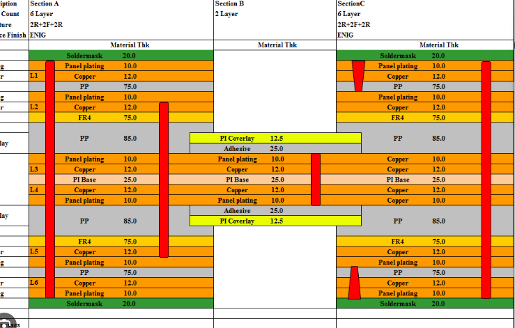
Transitioning to the next consideration, the layer configuration plays a pivotal role in the overall design.
A stack-up flex PCB can have multiple layers, each serving a specific function. The arrangement of these layers must be meticulously planned to balance electrical performance with mechanical flexibility. Signal integrity is a primary concern, necessitating careful routing of high-speed signals to minimize crosstalk and electromagnetic interference. Ground and power planes should be strategically placed to provide a low-impedance path and reduce noise.
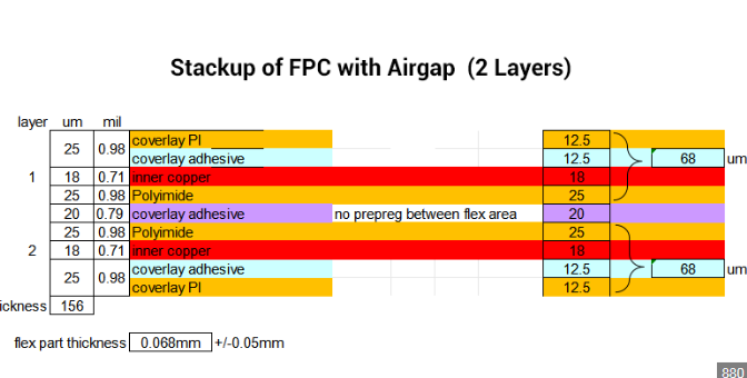
Another crucial factor is the bend radius, which directly impacts the durability of the flex PCB.
The bend radius is the minimum radius the flex PCB can be bent without causing damage. It is influenced by the thickness of the materials used and the number of layers in the stack-up. Designers must ensure that the bend radius is within acceptable limits to prevent cracking or delamination. Additionally, the placement of components and vias in bend areas should be avoided to reduce stress concentration.
Thermal management is another significant consideration in the design of stack-up flex PCBs.
The flexible nature of these PCBs can lead to challenges in dissipating heat, especially in high-power applications. Effective thermal management strategies, such as the use of thermal vias, heat sinks, and proper layer stack-up, are essential to maintain the reliability and performance of the PCB. The thermal conductivity of the materials used should also be evaluated to ensure efficient heat dissipation.
Moving on to the aspect of manufacturability, the design of stack-up flex PCBs must consider the capabilities and limitations of the fabrication process.
The choice of materials, layer count, and overall complexity can affect the manufacturability and cost of the PCB. Designers should work closely with manufacturers to ensure that the design can be produced reliably and cost-effectively. Design for manufacturability (DFM) guidelines should be followed to minimize potential issues during production.
Furthermore, the mechanical properties of the stack-up flex PCB must be evaluated to ensure it can withstand the intended application environment.
Factors such as tensile strength, elongation, and flexibility should be considered to ensure the PCB can endure mechanical stresses without failure. Environmental factors, including temperature, humidity, and exposure to chemicals, should also be taken into account during the design phase.
In conclusion, designing a stack-up flex PCB involves a comprehensive understanding of material properties, layer configuration, bend radius, thermal management, manufacturability, and mechanical properties. Each of these considerations plays a vital role in ensuring the performance, reliability, and longevity of the final product. By meticulously addressing these factors, designers can create stack-up flex PCBs that meet the stringent requirements of modern electronic applications.
Common Applications Of Stack Up Flex PCB In Industry
Stack up flex PCBs, or flexible printed circuit boards, have become increasingly prevalent in various industries due to their unique properties and versatile applications. These advanced circuit boards are designed to bend and flex, making them ideal for use in environments where traditional rigid PCBs would be impractical or impossible to implement. As technology continues to evolve, the demand for stack up flex PCBs has surged, driven by their ability to meet the stringent requirements of modern electronic devices and systems.
One of the most common applications of stack up flex PCBs is in the consumer electronics industry.
Devices such as smartphones, tablets, and wearable technology rely heavily on these flexible circuits to achieve their compact and lightweight designs. The ability of stack up flex PCBs to conform to the intricate shapes and contours of these devices allows manufacturers to maximize space efficiency while maintaining high performance. Additionally, the durability and reliability of these PCBs ensure that consumer electronics can withstand the rigors of daily use, including bending, twisting, and other mechanical stresses.
In the automotive industry, stack up flex PCBs play a crucial role in the development of advanced driver-assistance systems (ADAS) and other electronic components.
Modern vehicles are equipped with a multitude of sensors, cameras, and communication modules that require flexible and reliable interconnections. Stack up flex PCBs provide the necessary flexibility to integrate these components seamlessly into the vehicle’s design, enhancing both functionality and safety. Furthermore, the automotive sector benefits from the lightweight nature of these PCBs, which contributes to overall vehicle efficiency and performance.
The medical field also leverages the advantages of stack up flex PCBs in the design and manufacture of various medical devices.
From diagnostic equipment to wearable health monitors, these flexible circuits enable the creation of compact, portable, and highly reliable medical instruments. For instance, in minimally invasive surgical tools, stack up flex PCBs allow for the integration of complex electronic systems within small, flexible structures, facilitating precise and effective medical procedures. The biocompatibility and robustness of these PCBs further ensure that they can be safely used in medical applications without compromising patient safety.
Aerospace and defense industries are yet another domain where stack up flex PCBs find significant applications.
The stringent requirements for reliability, performance, and weight reduction in aerospace and defense systems make these flexible circuits an ideal choice. They are used in a variety of applications, including satellite systems, avionics, and military communication devices. The ability of stack up flex PCBs to withstand extreme environmental conditions, such as high temperatures and vibrations, ensures the reliability and longevity of critical aerospace and defense equipment.
Moreover, the industrial sector benefits from the use of stack up flex PCBs in automation and control systems.
Industrial machinery and robotics often require flexible and durable electronic interconnections to function efficiently. Stack up flex PCBs provide the necessary flexibility to accommodate the dynamic movements and complex configurations of these systems. Their resilience to harsh industrial environments, including exposure to chemicals and mechanical wear, further enhances their suitability for industrial applications.
In conclusion, stack up flex PCBs have become indispensable across a wide range of industries due to their unique properties and versatile applications. From consumer electronics and automotive systems to medical devices, aerospace, defense, and industrial automation, these flexible circuits offer unparalleled advantages in terms of design flexibility, reliability, and performance. As technology continues to advance, the adoption of stack up flex PCBs is expected to grow, driving innovation and efficiency in various sectors.
Manufacturing Process Of Stack Up Flex PCB
The manufacturing process of stack up flexible printed circuit boards (PCBs) is a sophisticated and intricate procedure that demands precision and expertise. This process begins with the selection of appropriate materials, which are crucial for ensuring the flexibility and durability of the final product. Typically, polyimide films are chosen due to their excellent thermal stability and mechanical properties. These films serve as the substrate upon which the circuit is built.
Once the substrate material is selected, the next step involves the application of a conductive layer, usually copper, onto the polyimide film.
This is achieved through a process known as lamination, where the copper foil is bonded to the substrate under heat and pressure. Following this, a photoresist layer is applied to the copper surface. The photoresist is a light-sensitive material that allows for the precise patterning of the circuit design.
Subsequently, the photoresist-coated substrate undergoes a process called photolithography.
During this stage, the substrate is exposed to ultraviolet light through a mask that contains the desired circuit pattern. The areas of the photoresist exposed to the light harden, while the unexposed areas remain soft and can be washed away using a developer solution. This leaves behind a patterned photoresist layer that corresponds to the circuit design.
The next phase involves etching, where the exposed copper areas are removed using a chemical solution, leaving behind the copper traces that form the circuit. After etching, the remaining photoresist is stripped away, revealing the copper circuit on the polyimide substrate. To protect the circuit and enhance its durability, a solder mask is applied. This insulating layer covers the entire surface except for the areas where components will be soldered.
Following the application of the solder mask, the stack-up process begins.
This involves layering multiple flexible circuits together to form a multi-layer flex PCB. Each layer is carefully aligned and bonded using adhesive materials. The bonding process is critical, as it ensures the electrical connectivity and mechanical integrity of the final product. Heat and pressure are applied to cure the adhesive and secure the layers together.
Once the layers are bonded, the stack-up undergoes drilling to create vias, which are small holes that allow electrical connections between different layers. These vias are then plated with copper to ensure conductivity. The final step in the manufacturing process is the application of surface finishes, such as gold or silver, to the exposed copper areas. These finishes protect the copper from oxidation and provide a reliable surface for soldering components.
Throughout the entire manufacturing process, rigorous quality control measures are implemented to ensure the final product meets the required specifications. This includes visual inspections, electrical testing, and reliability testing to verify the performance and durability of the stack-up flex PCB.
In conclusion, the manufacturing process of stack-up flexible PCBs is a complex and meticulous procedure that involves multiple stages, from material selection to final testing. Each step is crucial in ensuring the flexibility, durability, and reliability of the final product. By adhering to stringent quality control measures and utilizing advanced manufacturing techniques, manufacturers can produce high-quality stack-up flex PCBs that meet the demands of various applications in industries such as aerospace, medical devices, and consumer electronics.