Smt pcba
Benefits Of SMT PCBA In Modern Electronics
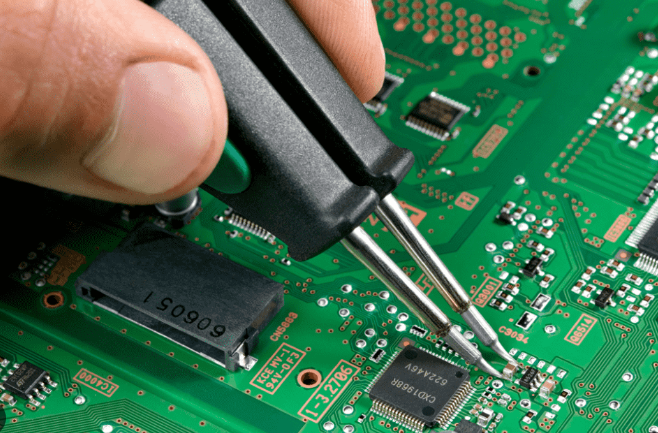
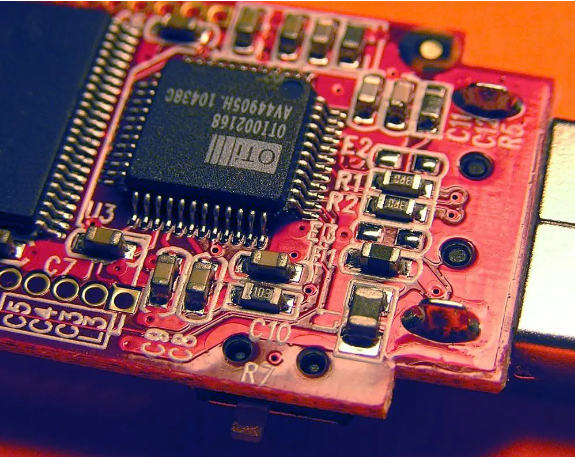
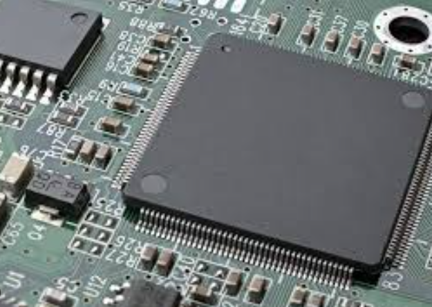
Surface Mount Technology (SMT) Printed Circuit Board Assembly (PCBA) has revolutionized the electronics industry, offering numerous advantages that have made it the preferred method for assembling electronic components.
One of the primary benefits of SMT PCBA is its ability to significantly reduce the size and weight of electronic devices.
By allowing components to be mounted directly onto the surface of the PCB, SMT eliminates the need for through-hole connections, which traditionally required more space and added weight. This miniaturization is crucial in the development of modern electronics, where compactness and portability are highly valued.
In addition to size and weight reduction, SMT PCBA enhances the performance and reliability of electronic devices.
The shorter electrical paths in SMT assemblies result in lower inductance and resistance, which in turn leads to improved signal integrity and faster signal transmission. This is particularly important in high-frequency applications where signal degradation can be a critical issue. Furthermore, the robust mechanical connections formed during the reflow soldering process in SMT ensure that components are securely attached to the PCB, reducing the likelihood of mechanical failure due to vibration or thermal cycling.
Another significant advantage of SMT PCBA is its cost-effectiveness.
The automation of the SMT assembly process allows for high-speed production with minimal human intervention, leading to lower labor costs and increased production efficiency. Automated pick-and-place machines can accurately position thousands of components per hour, significantly reducing assembly time compared to manual through-hole assembly. Additionally, the ability to place components on both sides of the PCB further optimizes space utilization and reduces material costs.
The versatility of SMT PCBA also contributes to its widespread adoption in various industries.
SMT can accommodate a wide range of component types, including resistors, capacitors, integrated circuits, and more. This flexibility allows designers to create complex and multifunctional electronic devices that meet the diverse needs of different applications. Moreover, the compatibility of SMT with advanced manufacturing techniques, such as flexible PCBs and high-density interconnects (HDI), enables the development of innovative products that push the boundaries of technology.
Environmental considerations also play a role in the growing preference for SMT PCBA.
The reduced material usage and waste generation associated with SMT assembly align with the principles of sustainable manufacturing. Additionally, the lead-free soldering processes commonly used in SMT are compliant with environmental regulations, such as the Restriction of Hazardous Substances (RoHS) directive, which aims to minimize the environmental impact of electronic waste.
In conclusion, the benefits of SMT PCBA in modern electronics are manifold, encompassing size and weight reduction, enhanced performance and reliability, cost-effectiveness, versatility, and environmental sustainability. As technology continues to advance, the demand for smaller, faster, and more efficient electronic devices will only increase, further solidifying the importance of SMT PCBA in the electronics industry. By leveraging the advantages of SMT, manufacturers can meet the evolving needs of consumers and stay competitive in a rapidly changing market.

Common Challenges In SMT PCBA Manufacturing
Surface Mount Technology (SMT) in Printed Circuit Board Assembly (PCBA) has revolutionized the electronics manufacturing industry by enabling the production of smaller, more efficient, and highly reliable electronic devices. However, despite its numerous advantages, SMT PCBA manufacturing is not without its challenges. Understanding these common challenges is crucial for manufacturers aiming to optimize their production processes and ensure high-quality outcomes.
One of the primary challenges in SMT PCBA manufacturing is component placement accuracy.
As electronic devices become increasingly compact, the components used in these devices also shrink in size. This miniaturization necessitates precise placement of components on the PCB. Even a slight misalignment can lead to functional failures or reduced performance of the final product. Advanced placement machines and meticulous calibration are essential to mitigate this issue, but they also add to the complexity and cost of the manufacturing process.
Another significant challenge is solder paste application.
Solder paste serves as the adhesive that holds components in place and ensures electrical connectivity. The application process must be meticulously controlled to achieve the correct volume and placement of solder paste. Inconsistent application can result in defects such as solder bridges, insufficient solder joints, or tombstoning, where components stand on end rather than lying flat. To address this, manufacturers often employ automated stencil printers and rigorous inspection systems, yet these solutions require substantial investment and maintenance.
Thermal management during the reflow soldering process presents another hurdle.
Reflow soldering involves heating the entire PCB assembly to melt the solder paste and form reliable solder joints. However, different components on the PCB may have varying thermal sensitivities and mass, leading to uneven heating. This can cause issues such as cold solder joints or thermal damage to sensitive components. Manufacturers must carefully design their thermal profiles and may need to use multiple heating zones to ensure uniform temperature distribution, adding another layer of complexity to the process.
Component availability and supply chain management also pose significant challenges.
the electronics industry is highly dynamic, with rapid advancements and frequent changes in component specifications. Ensuring a steady supply of the required components can be difficult, especially during periods of high demand or global supply chain disruptions. Manufacturers must maintain strong relationships with suppliers and often need to have contingency plans in place to mitigate the impact of component shortages.
Quality control is another critical aspect that cannot be overlooked.
Detecting and addressing defects early in the manufacturing process is essential to avoid costly rework or product recalls. Automated optical inspection (AOI) and X-ray inspection systems are commonly used to identify defects such as misaligned components, soldering issues, and hidden faults. However, these systems require significant investment and skilled operators to interpret the results accurately.
Finally, the rapid pace of technological advancements in the electronics industry means that manufacturers must continuously adapt and upgrade their equipment and processes.
Staying competitive requires ongoing investment in new technologies and training for personnel. This constant need for innovation can strain resources and necessitate careful planning and strategic decision-making.
In conclusion, while SMT PCBA manufacturing offers numerous benefits, it also presents a range of challenges that manufacturers must navigate. From component placement accuracy and solder paste application to thermal management, supply chain issues, quality control, and the need for continuous innovation, each challenge requires careful consideration and strategic solutions. By understanding and addressing these challenges, manufacturers can enhance their production processes, ensuring the delivery of high-quality electronic products in an increasingly competitive market.

Innovations In SMT PCBA Technology
Surface Mount Technology (SMT) and Printed Circuit Board Assembly (PCBA) have undergone significant advancements in recent years, revolutionizing the electronics manufacturing industry. These innovations have not only enhanced the efficiency and precision of the assembly process but have also paved the way for the development of more compact and complex electronic devices. As the demand for smaller, faster, and more reliable electronics continues to grow, the importance of SMT PCBA technology cannot be overstated.
One of the most notable innovations in SMT PCBA technology is the development of advanced placement machines.
These machines are capable of placing components with incredible accuracy and speed, significantly reducing the time required for assembly. Modern placement machines utilize sophisticated vision systems and algorithms to ensure that each component is placed precisely where it needs to be, minimizing the risk of errors and improving overall yield. Additionally, these machines can handle a wide range of component sizes and types, making them highly versatile and adaptable to various manufacturing needs.
Another significant advancement in SMT PCBA technology is the introduction of lead-free soldering processes.
Traditional soldering methods often relied on lead-based solders, which posed environmental and health risks. In response to these concerns, the industry has shifted towards lead-free alternatives, such as tin-silver-copper (SAC) alloys. These lead-free solders not only meet stringent environmental regulations but also offer improved mechanical and thermal properties, ensuring the reliability and longevity of electronic assemblies.
Furthermore, the integration of automated optical inspection (AOI) systems has greatly enhanced the quality control process in SMT PCBA manufacturing.
AOI systems use high-resolution cameras and advanced image processing techniques to inspect assembled PCBs for defects, such as misaligned components, solder bridges, and insufficient solder joints. By identifying and addressing these issues early in the production process, manufacturers can significantly reduce the likelihood of defective products reaching the market, thereby improving customer satisfaction and reducing warranty costs.
In addition to these technological advancements, the adoption of Industry 4.0 principles has also had a profound impact on SMT PCBA manufacturing.
Industry 4.0, characterized by the integration of cyber-physical systems, the Internet of Things (IoT), and big data analytics, has enabled manufacturers to achieve unprecedented levels of automation, connectivity, and data-driven decision-making. For instance, real-time monitoring and predictive maintenance systems can help identify potential equipment failures before they occur, minimizing downtime and maximizing productivity. Moreover, the use of digital twins – virtual replicas of physical assets – allows manufacturers to simulate and optimize production processes, leading to more efficient and cost-effective operations.
The continuous miniaturization of electronic components has also driven innovations in SMT PCBA technology.
As devices become smaller and more complex, the need for high-density interconnect (HDI) PCBs has increased. HDI PCBs feature finer traces, smaller vias, and more layers, enabling the integration of more components in a limited space. Advanced fabrication techniques, such as laser drilling and sequential lamination, have been developed to meet the stringent requirements of HDI PCBs, ensuring their reliability and performance.
In conclusion, the innovations in SMT PCBA technology have significantly transformed the electronics manufacturing landscape. From advanced placement machines and lead-free soldering processes to automated optical inspection systems and Industry 4.0 integration, these advancements have enhanced the efficiency, precision, and quality of electronic assemblies. As the demand for smaller, faster, and more reliable devices continues to grow, the importance of staying at the forefront of SMT PCBA technology will only become more critical for manufacturers seeking to maintain a competitive edge in the market.

Quality Control Techniques For SMT PCBA
Surface Mount Technology (SMT) Printed Circuit Board Assembly (PCBA) is a critical process in modern electronics manufacturing, necessitating rigorous quality control techniques to ensure the reliability and performance of the final product. The complexity of SMT PCBA, characterized by the miniaturization of components and the precision required in their placement, demands a multifaceted approach to quality control. This article explores various quality control techniques employed in SMT PCBA, emphasizing their importance in maintaining high standards.
To begin with, Automated Optical Inspection (AOI) is a cornerstone of quality control in SMT PCBA.
AOI systems utilize high-resolution cameras to capture images of the assembled PCB, which are then analyzed to detect defects such as misaligned components, soldering issues, and missing parts. The non-contact nature of AOI allows for rapid inspection without risking damage to the delicate components. By identifying defects early in the production process, AOI helps in reducing rework costs and improving overall yield.
In addition to AOI, X-ray inspection is another vital technique, particularly for detecting hidden defects in solder joints and components.
X-ray inspection systems can penetrate through layers of the PCB, providing a detailed view of the internal structure. This is especially useful for inspecting Ball Grid Array (BGA) components, where traditional optical methods fall short. By revealing issues such as voids, solder bridges, and insufficient solder, X-ray inspection ensures the integrity of connections that are crucial for the functionality of the PCB.
Furthermore, In-Circuit Testing (ICT) plays a significant role in verifying the electrical performance of the assembled PCB.
ICT involves the use of a bed-of-nails fixture to make contact with various test points on the PCB, allowing for the measurement of electrical parameters such as resistance, capacitance, and signal integrity. This technique is highly effective in identifying issues like open circuits, short circuits, and incorrect component values. By ensuring that each circuit functions as intended, ICT contributes to the overall reliability of the final product.
Complementing ICT, Functional Testing (FT) is employed to simulate the operational environment of the PCB and verify its performance under real-world conditions.
Functional testing involves applying power to the PCB and running software or firmware to check for proper operation. This technique helps in identifying issues that may not be apparent during static testing, such as thermal performance, signal timing, and interaction between components. By validating the PCB’s functionality in a dynamic environment, functional testing provides an additional layer of assurance.
Moreover, Statistical Process Control (SPC) is an essential technique for monitoring and controlling the manufacturing process.
SPC involves the collection and analysis of data from various stages of production to identify trends and variations. By using control charts and other statistical tools, manufacturers can detect deviations from the norm and take corrective actions before defects occur. This proactive approach helps in maintaining consistent quality and reducing the likelihood of defects.
Lastly, Environmental Stress Screening (ESS) is employed to expose the assembled PCB to extreme conditions such as temperature cycling, vibration, and humidity. ESS aims to identify latent defects that may not manifest under normal conditions but could lead to failures in the field. By subjecting the PCB to accelerated aging, ESS helps in ensuring long-term reliability and robustness.
In conclusion, the quality control techniques for SMT PCBA are diverse and multifaceted, each addressing different aspects of the manufacturing process. From visual inspections to electrical testing and environmental screening, these techniques collectively ensure that the final product meets the highest standards of quality and reliability. By implementing these rigorous quality control measures, manufacturers can deliver PCBs that perform reliably in a wide range of applications, thereby meeting the ever-increasing demands of the electronics industry.
