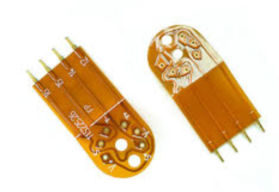
Sculptured flex pcb
Advantages Of Sculptured Flex PCB In Modern Electronics
Sculptured flex PCBs, or sculptured flexible printed circuit boards, have emerged as a transformative technology in the realm of modern electronics. These advanced circuit boards offer a multitude of advantages that make them highly desirable for a wide range of applications.
One of the most significant benefits of sculptured flex PCBs is their inherent flexibility.
Unlike traditional rigid PCBs, sculptured flex PCBs can be bent, twisted, and folded without compromising their functionality. This flexibility allows for innovative design possibilities, enabling the creation of compact and lightweight electronic devices that can fit into unconventional spaces.
In addition to their flexibility, sculptured flex PCBs are known for their durability.
The materials used in their construction are typically more resilient to environmental stressors such as vibration, shock, and temperature fluctuations. This makes them ideal for use in harsh environments where traditional PCBs might fail. Furthermore, the ability to withstand repeated bending and flexing without damage extends the lifespan of devices that incorporate these advanced circuit boards.
Another notable advantage of sculptured flex PCBs is their ability to reduce the overall weight and size of electronic devices.
By integrating multiple layers of circuitry into a single flexible substrate, these PCBs eliminate the need for bulky connectors and wiring. This not only streamlines the design but also enhances the performance of the device by reducing signal loss and improving electrical efficiency. Consequently, sculptured flex PCBs are particularly beneficial in applications where space and weight are critical factors, such as in aerospace, medical devices, and wearable technology.
Moreover, the manufacturing process of sculptured flex PCBs offers significant cost savings.
The ability to produce complex circuits on a single flexible substrate reduces the need for multiple rigid boards and interconnecting components. This simplification of the assembly process leads to lower production costs and shorter lead times. Additionally, the use of advanced materials and manufacturing techniques ensures high reliability and consistency in the final product, further contributing to cost efficiency.
The versatility of sculptured flex PCBs also extends to their application in dynamic and moving parts.
For instance, in robotics and automotive industries, these PCBs can be used in joints and hinges where constant movement is required. The flexibility and durability of sculptured flex PCBs ensure that they can withstand continuous motion without failure, thereby enhancing the reliability and longevity of the devices in which they are used.
Furthermore, sculptured flex PCBs contribute to improved thermal management in electronic devices.
The flexible nature of these PCBs allows for better heat dissipation, which is crucial in high-performance applications where overheating can be a significant concern. By efficiently managing heat, sculptured flex PCBs help maintain optimal operating temperatures, thereby enhancing the performance and reliability of electronic devices.
In conclusion, the advantages of sculptured flex PCBs in modern electronics are manifold. Their flexibility, durability, and ability to reduce weight and size make them indispensable in a variety of applications. The cost savings associated with their manufacturing process, coupled with their versatility and improved thermal management, further underscore their value. As technology continues to advance, the adoption of sculptured flex PCBs is likely to increase, driving innovation and enabling the development of more sophisticated and reliable electronic devices.

Design Techniques For Sculptured Flex PCB
Sculptured flex PCBs, a specialized subset of flexible printed circuit boards, offer unique advantages in applications requiring three-dimensional configurations and dynamic flexing. The design techniques for sculptured flex PCBs are intricate and demand a thorough understanding of both material properties and advanced fabrication processes. To achieve optimal performance and reliability, designers must consider several critical factors, including material selection, layer stack-up, trace routing, and mechanical reinforcement.
Material selection is paramount in sculptured flex PCB design.
The choice of substrate, typically polyimide, must balance flexibility, thermal stability, and mechanical strength. Polyimide’s excellent thermal resistance and flexibility make it a preferred choice, but designers must also consider the adhesive systems used to bond the layers. Adhesives must be chosen to withstand the thermal and mechanical stresses encountered during both the manufacturing process and the operational life of the PCB. Additionally, the copper foil used for the conductive traces must be carefully selected to ensure it can endure repeated flexing without cracking or delaminating.
Layer stack-up is another crucial aspect of sculptured flex PCB design.
The stack-up must be meticulously planned to ensure that the PCB can bend and flex as required without compromising electrical performance or mechanical integrity. This involves determining the optimal number of layers, the thickness of each layer, and the placement of stiffeners or other mechanical supports. The use of stiffeners, typically made from materials such as FR4 or stainless steel, can provide additional rigidity in specific areas while allowing flexibility in others. This selective reinforcement is essential for maintaining the structural integrity of the PCB in applications where it must endure repeated bending or twisting.
Trace routing in sculptured flex PCBs requires careful consideration to minimize stress on the conductive paths.
Designers must avoid sharp bends and ensure that traces are routed with smooth, gradual curves to distribute mechanical stress evenly. Additionally, the width and spacing of traces must be optimized to prevent issues such as signal degradation, crosstalk, and electromagnetic interference. The use of ground planes and shielding can further enhance signal integrity, particularly in high-frequency applications. Moreover, designers must account for the potential impact of the flexing motion on the electrical performance of the traces, ensuring that the PCB can maintain reliable connectivity throughout its operational life.
Mechanical reinforcement is often necessary to enhance the durability of sculptured flex PCBs.
This can be achieved through the strategic placement of stiffeners, as previously mentioned, or by incorporating additional layers of protective materials such as coverlays or encapsulants. These materials can shield the delicate conductive traces from environmental factors such as moisture, dust, and mechanical abrasion. Furthermore, the use of strain relief features, such as fillets or teardrops at the junctions of traces and pads, can help distribute mechanical stress and prevent cracking or delamination.
In conclusion, the design techniques for sculptured flex PCBs are multifaceted and require a comprehensive understanding of material properties, fabrication processes, and mechanical dynamics. By carefully selecting materials, planning the layer stack-up, optimizing trace routing, and incorporating mechanical reinforcement, designers can create robust and reliable sculptured flex PCBs that meet the demanding requirements of modern electronic applications. These advanced design techniques ensure that sculptured flex PCBs can deliver exceptional performance and durability, even in the most challenging environments.
Applications Of Sculptured Flex PCB In Wearable Technology
Sculptured flex PCBs, or sculptured flexible printed circuit boards, represent a significant advancement in the realm of electronic design, particularly within the burgeoning field of wearable technology. These innovative circuit boards are characterized by their unique three-dimensional structures, which allow for greater flexibility and adaptability compared to traditional rigid or even standard flexible PCBs
. As wearable technology continues to evolve, the applications of sculptured flex PCBs are becoming increasingly prominent, offering numerous advantages that enhance both functionality and user experience.
One of the primary applications of sculptured flex PCBs in wearable technology is in the development of smart clothing.
Smart clothing integrates electronic components directly into the fabric, enabling functionalities such as health monitoring, fitness tracking, and even communication. The inherent flexibility of sculptured flex PCBs makes them ideal for this purpose, as they can conform to the contours of the human body without compromising performance. This adaptability ensures that the electronic components remain unobtrusive and comfortable for the wearer, a critical factor in the widespread adoption of smart clothing.
In addition to smart clothing, sculptured flex PCBs are also finding applications in wearable medical devices.
These devices, which include heart rate monitors, glucose sensors, and other health tracking tools, require a high degree of precision and reliability. The three-dimensional nature of sculptured flex PCBs allows for more complex and compact designs, which can be crucial in creating devices that are both effective and discreet. Furthermore, the flexibility of these PCBs ensures that the devices can be worn comfortably for extended periods, thereby improving patient compliance and the overall effectiveness of the monitoring.
Moreover, the use of sculptured flex PCBs extends to the realm of wearable fitness technology.
Fitness trackers and smartwatches are becoming increasingly sophisticated, incorporating a wide range of sensors and functionalities. The compact and flexible design of sculptured flex PCBs enables the integration of multiple components within a single device, enhancing its capabilities without increasing its size or weight. This is particularly important for fitness enthusiasts who require lightweight and durable devices that can withstand rigorous physical activity.
Transitioning to another significant application, sculptured flex PCBs are also being utilized in the development of augmented reality (AR) and virtual reality (VR) headsets.
These headsets demand high-performance electronic components that can deliver immersive experiences while maintaining a lightweight and comfortable form factor. Sculptured flex PCBs provide the necessary flexibility and compactness, allowing for the integration of advanced sensors, displays, and processing units within the limited space of a headset. This not only improves the overall user experience but also opens up new possibilities for the design and functionality of AR and VR devices.
Furthermore, the potential of sculptured flex PCBs in wearable technology is not limited to current applications.
As the technology continues to advance, new and innovative uses are likely to emerge. For instance, the integration of sculptured flex PCBs in wearable robotics and exoskeletons could revolutionize the field, providing enhanced mobility and support for individuals with physical disabilities. The adaptability and versatility of these PCBs make them a promising component in the ongoing development of next-generation wearable technologies.
In conclusion, sculptured flex PCBs are playing a pivotal role in the advancement of wearable technology. Their unique three-dimensional structures and inherent flexibility offer significant advantages in terms of design, functionality, and user comfort. From smart clothing and medical devices to fitness trackers and AR/VR headsets, the applications of sculptured flex PCBs are diverse and continually expanding. As technology progresses, these innovative circuit boards are set to become an integral part of the wearable technology landscape, driving further innovation and enhancing the capabilities of wearable devices.
Manufacturing Challenges And Solutions For Sculptured Flex PCB
Sculptured flex PCBs, with their unique three-dimensional structures, offer significant advantages in terms of flexibility, space-saving, and integration capabilities. However, the manufacturing of these advanced circuit boards presents a series of challenges that require innovative solutions to ensure reliability and performance. One of the primary challenges in the production of sculptured flex PCBs is the precise control of the material properties. The flexible substrates used in these PCBs must maintain their integrity under mechanical stress while providing the necessary electrical performance. This necessitates the use of high-quality polyimide films or other flexible materials that can withstand bending and twisting without compromising the circuit’s functionality. Additionally, the adhesion between the conductive layers and the substrate must be robust to prevent delamination during use.
Another significant challenge is the accurate patterning of the conductive traces on the flexible substrate. Traditional photolithography techniques, commonly used in rigid PCB manufacturing, may not be directly applicable due to the flexible nature of the substrate. Therefore, advanced techniques such as laser direct imaging (LDI) or inkjet printing are often employed to achieve the required precision. These methods allow for the creation of fine features and complex geometries that are essential for the functionality of sculptured flex PCBs. However, they also demand stringent process control and calibration to ensure consistency and repeatability.
Thermal management is another critical aspect that poses challenges in the manufacturing of sculptured flex PCBs.
The flexible substrates typically have lower thermal conductivity compared to rigid materials, which can lead to heat accumulation and potential damage to the components. To address this issue, manufacturers often incorporate thermal vias or use thermally conductive adhesives to enhance heat dissipation. Additionally, careful design considerations, such as optimizing the placement of heat-generating components and using thermal reliefs, are essential to mitigate thermal stress.
The assembly process of sculptured flex PCBs also presents unique challenges.
The three-dimensional nature of these PCBs requires specialized equipment and techniques for component placement and soldering. Traditional pick-and-place machines may not be suitable for handling the flexible substrates, necessitating the use of custom fixtures or robotic systems. Furthermore, the soldering process must be carefully controlled to prevent thermal damage to the flexible substrate and ensure reliable connections. Techniques such as reflow soldering with controlled temperature profiles or the use of low-temperature solder alloys are often employed to achieve this.
Quality control and testing of sculptured flex PCBs are equally challenging due to their complex geometries and flexible nature.
Standard inspection methods, such as automated optical inspection (AOI) or X-ray inspection, may need to be adapted to accommodate the three-dimensional structures. Additionally, electrical testing must account for the potential variations in resistance and capacitance introduced by the flexible substrate. Advanced testing methods, such as flying probe testing or flexible test fixtures, are often used to ensure the functionality and reliability of the final product.
In conclusion, the manufacturing of sculptured flex PCBs involves a series of challenges that require innovative solutions and advanced techniques. From material selection and patterning to thermal management and assembly, each step of the process demands careful consideration and precise control. By addressing these challenges, manufacturers can harness the benefits of sculptured flex PCBs, enabling the development of compact, flexible, and high-performance electronic devices.