Rf pcb layout guidelines
Best Practices For RF PCB Layout Design
Designing a printed circuit board (PCB) for radio frequency (RF) applications requires meticulous attention to detail and adherence to specific guidelines to ensure optimal performance.
The complexity of RF signals, which operate at high frequencies, necessitates a thorough understanding of electromagnetic principles and careful planning to mitigate issues such as signal loss, interference, and impedance mismatches. Consequently, implementing best practices for RF PCB layout design is crucial for achieving reliable and efficient operation.
To begin with, one of the fundamental aspects of RF PCB layout design is the selection of appropriate materials.
The dielectric constant and loss tangent of the substrate material significantly influence signal integrity. Low-loss materials, such as Rogers or Teflon-based substrates, are often preferred over standard FR4 due to their superior high-frequency performance. Additionally, the thickness of the substrate should be chosen to balance mechanical stability and electrical performance, ensuring minimal signal degradation.
Transitioning to the layout itself, the placement of components is paramount.
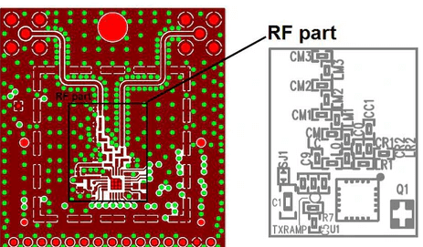
RF components, such as amplifiers, mixers, and filters, should be positioned to minimize the length of signal paths. Shorter signal paths reduce the potential for signal loss and crosstalk. Furthermore, sensitive components should be isolated from noisy digital circuits to prevent electromagnetic interference (EMI). Shielding techniques, such as ground planes and metal enclosures, can be employed to further protect sensitive areas from external noise sources.
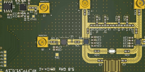
Another critical consideration is the design of transmission lines. Microstrip and stripline configurations are commonly used for RF signal routing.
The characteristic impedance of these transmission lines must be carefully controlled to match the impedance of the source and load, typically 50 ohms. Impedance mismatches can lead to signal reflections and loss, degrading overall performance. To achieve precise impedance control, the width of the transmission lines and the spacing to the ground plane must be accurately calculated and maintained throughout the layout.
Moreover, grounding is a vital aspect of RF PCB design.
A solid and continuous ground plane is essential for providing a low-impedance return path for RF signals. This helps to minimize ground loops and reduce EMI. Vias should be strategically placed to connect the ground plane on different layers, ensuring a consistent ground potential across the board. Additionally, decoupling capacitors should be placed close to power pins of active components to filter out high-frequency noise and stabilize the power supply.
Thermal management is another important factor to consider.
RF components can generate significant heat, which, if not properly managed, can affect performance and reliability. Heat sinks, thermal vias, and proper airflow should be incorporated into the design to dissipate heat effectively. Ensuring adequate thermal management helps maintain the integrity of the RF signals and prolongs the lifespan of the components.
In conclusion, designing an RF PCB layout requires a comprehensive approach that encompasses material selection, component placement, transmission line design, grounding, and thermal management. By adhering to these best practices, designers can mitigate common issues associated with high-frequency signals and achieve a robust and efficient RF PCB. The meticulous application of these guidelines ensures that the final product meets the stringent performance requirements of modern RF applications, paving the way for reliable and high-quality communication systems.

Minimizing Signal Interference In RF PCB Layouts
Minimizing signal interference in RF PCB layouts is a critical aspect of designing high-performance radio frequency circuits. The complexity of RF signals, which operate at high frequencies, necessitates meticulous attention to detail in the layout process to ensure signal integrity and minimize interference.
One of the primary considerations in RF PCB layout is the careful management of signal paths.
Ensuring that signal traces are as short and direct as possible helps to reduce the potential for signal degradation and crosstalk. Additionally, maintaining consistent trace widths and avoiding abrupt changes in direction can further enhance signal integrity.
Another crucial factor is the use of proper grounding techniques. A well-designed ground plane can significantly reduce electromagnetic interference (EMI) and provide a stable reference point for signal return paths. It is essential to ensure that the ground plane is continuous and unbroken, as gaps or discontinuities can create unwanted inductance and capacitance, leading to signal distortion. Moreover, placing ground vias strategically around critical components and along signal paths can help to minimize ground loop areas and further reduce EMI.
Shielding is also an effective method for minimizing signal interference in RF PCB layouts.
By enclosing sensitive components and signal traces within grounded metal shields, designers can prevent external electromagnetic fields from coupling into the circuit. This is particularly important in environments with high levels of ambient RF noise. Additionally, shielding can help to contain any radiated emissions from the circuit itself, preventing it from interfering with other nearby electronic devices.
The placement of components on the PCB is another vital consideration.
Grouping related components together and placing them in close proximity can help to minimize the length of signal paths and reduce the potential for interference. For instance, placing decoupling capacitors as close as possible to the power pins of active components can help to filter out high-frequency noise and provide a stable power supply. Similarly, keeping high-speed signal traces away from sensitive analog components can prevent unwanted coupling and signal degradation.
Furthermore, the use of differential signaling can be beneficial in minimizing signal interference.
Differential pairs, which consist of two complementary signals, are less susceptible to common-mode noise and can provide improved signal integrity over long distances. Ensuring that differential pairs are routed together with consistent spacing and length matching is essential to maintain their noise-canceling properties.
In addition to these layout techniques, careful consideration of the PCB material and stack-up is necessary.
High-frequency signals can be affected by the dielectric properties of the PCB material, so selecting a material with low loss and stable dielectric constant is important. Moreover, a well-designed stack-up with appropriate layer assignments can help to control impedance and reduce signal reflections.
Finally, simulation and testing play a crucial role in minimizing signal interference in RF PCB layouts.
Using simulation tools to model the behavior of the circuit and identify potential sources of interference can help designers make informed decisions during the layout process. Once the PCB is fabricated, thorough testing and validation are necessary to ensure that the design meets performance specifications and operates reliably in its intended environment.
In conclusion, minimizing signal interference in RF PCB layouts requires a comprehensive approach that encompasses careful signal path management, effective grounding and shielding techniques, strategic component placement, the use of differential signaling, appropriate material selection, and rigorous simulation and testing. By adhering to these guidelines, designers can achieve high-performance RF circuits with robust signal integrity and minimal interference.
Importance Of Grounding In RF PCB Layouts
In the realm of RF PCB layouts, grounding plays a pivotal role in ensuring the optimal performance and reliability of the circuit. The importance of grounding cannot be overstated, as it serves as the foundation for minimizing noise, reducing electromagnetic interference (EMI), and maintaining signal integrity. To fully appreciate the significance of grounding in RF PCB layouts, it is essential to delve into the various aspects that contribute to its criticality.
Firstly, grounding provides a common reference point for all signals within the circuit.
This common reference is crucial for maintaining consistent signal levels and preventing potential differences that could lead to signal distortion or loss. By establishing a solid ground plane, designers can ensure that all components within the RF PCB share the same reference voltage, thereby enhancing the overall stability of the circuit.
Moreover, grounding plays a vital role in minimizing noise and EMI.
In RF circuits, high-frequency signals are particularly susceptible to noise and interference, which can degrade performance and lead to erroneous operation. A well-designed ground plane acts as a shield, absorbing and dissipating unwanted noise and interference. This shielding effect is especially important in RF applications, where even minor disruptions can have significant consequences. By providing a low-impedance path to ground, the ground plane helps to isolate sensitive components from external noise sources, thereby preserving signal integrity.
In addition to noise reduction, grounding is essential for controlling return currents.
In RF circuits, return currents follow the path of least impedance, which is typically the ground plane. By providing a continuous and low-impedance ground plane, designers can ensure that return currents flow predictably and do not create unwanted loops or paths that could introduce noise or interference. This controlled return current path is crucial for maintaining the integrity of high-frequency signals and preventing signal degradation.
Furthermore, grounding is integral to the proper functioning of decoupling capacitors.
Decoupling capacitors are used to filter out high-frequency noise and provide a stable power supply to active components. For these capacitors to be effective, they must be connected to a low-impedance ground plane. A well-designed ground plane ensures that decoupling capacitors can efficiently filter out noise and provide a stable power supply, thereby enhancing the overall performance of the RF circuit.
Another critical aspect of grounding in RF PCB layouts is the prevention of ground loops.
Ground loops occur when there are multiple ground paths with different potentials, leading to unwanted current flow and interference. By carefully designing the ground plane and ensuring a single, continuous ground path, designers can eliminate ground loops and prevent associated issues. This meticulous attention to grounding helps to maintain the integrity of the RF signals and ensures reliable circuit operation.
In conclusion, grounding is a fundamental aspect of RF PCB layout design that significantly impacts the performance and reliability of the circuit. By providing a common reference point, minimizing noise and EMI, controlling return currents, supporting decoupling capacitors, and preventing ground loops, a well-designed ground plane is essential for maintaining signal integrity and ensuring the optimal operation of RF circuits. As such, designers must prioritize grounding in their RF PCB layouts to achieve the best possible performance and reliability.
Techniques For Optimizing RF PCB Trace Routing
When designing RF PCB layouts, optimizing trace routing is crucial to ensure signal integrity and minimize interference. One of the primary techniques involves maintaining consistent trace impedance. This can be achieved by carefully controlling the trace width and the distance between the trace and the reference plane. By doing so, designers can prevent signal reflections and maintain signal quality. Additionally, using a controlled impedance calculator can help in determining the appropriate trace dimensions for a given substrate material and thickness.
Another essential technique is to minimize the length of RF traces.
Shorter traces reduce the potential for signal loss and radiation, which is particularly important at higher frequencies. To achieve this, designers should place RF components as close to each other as possible, thereby reducing the trace length and the associated parasitic inductance and capacitance. Furthermore, employing a star routing topology, where each RF component is connected directly to a central node, can help in minimizing trace lengths and ensuring equal signal distribution.
Incorporating proper grounding practices is also vital for optimizing RF PCB trace routing.
A solid ground plane provides a low-impedance return path for RF signals, reducing the risk of ground loops and electromagnetic interference (EMI). Designers should ensure that the ground plane is continuous and unbroken, avoiding any slots or gaps that could disrupt the return path. Additionally, using multiple ground vias to connect the ground plane to the top and bottom layers of the PCB can further enhance signal integrity by providing a robust grounding network.
Shielding is another technique that can significantly improve RF PCB performance.
By enclosing sensitive RF traces and components within a grounded metal shield, designers can protect them from external EMI and prevent them from radiating unwanted signals. This is particularly important in mixed-signal designs, where digital and analog circuits coexist on the same PCB. In such cases, careful partitioning of the PCB layout, with separate ground planes for digital and analog sections, can help in minimizing crosstalk and interference.
Moreover, the use of differential signaling can be beneficial in RF PCB designs.
Differential pairs, consisting of two traces carrying equal and opposite signals, can help in reducing common-mode noise and improving signal integrity. To ensure optimal performance, designers should maintain a consistent spacing between the differential traces and route them symmetrically. This helps in preserving the balance of the differential signals and minimizing any potential skew.
In addition to these techniques, proper termination of RF traces is essential to prevent signal reflections and ensure signal integrity.
Impedance matching between the source, trace, and load can be achieved using various termination methods, such as series or parallel resistors, or more complex matching networks. By carefully selecting the appropriate termination components and placing them close to the source or load, designers can effectively minimize signal reflections and maintain signal quality.
Lastly, simulation and analysis tools play a crucial role in optimizing RF PCB trace routing. Electromagnetic simulation software can help designers visualize the behavior of RF signals on the PCB and identify potential issues, such as signal reflections, crosstalk, and EMI. By iterating through the design process and making necessary adjustments based on simulation results, designers can achieve an optimized RF PCB layout that meets performance requirements.
In conclusion, optimizing RF PCB trace routing involves a combination of techniques, including maintaining consistent trace impedance, minimizing trace length, incorporating proper grounding practices, using shielding, employing differential signaling, ensuring proper termination, and leveraging simulation tools. By carefully considering these factors, designers can create RF PCB layouts that deliver superior performance and reliability.