Quick pcb prototyping
Essential Tools For Quick PCB Prototyping
Quick PCB prototyping is an essential process in the development of electronic devices, allowing engineers and designers to test and refine their circuit designs before committing to full-scale production. To achieve efficient and effective prototyping, a variety of tools are indispensable. These tools not only streamline the design process but also ensure accuracy and reliability in the final product.
First and foremost, a robust PCB design software is crucial.
Software such as Altium Designer, Eagle, or KiCad provides a comprehensive suite of tools for schematic capture, layout design, and simulation. These programs enable designers to create detailed circuit diagrams, place components accurately, and route connections efficiently. Additionally, they often include libraries of pre-designed components, which can save significant time and reduce the likelihood of errors. The ability to simulate the circuit before physical prototyping is another invaluable feature, allowing for the identification and correction of potential issues early in the design process.
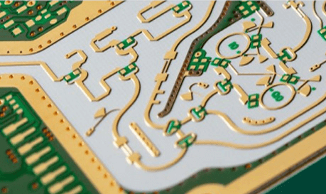
Once the design is complete, the next essential tool is a high-quality PCB printer or milling machine.
These devices translate the digital design into a physical prototype. PCB printers, such as those using inkjet or laser technology, can produce precise and intricate circuit patterns on various substrates. Alternatively, milling machines, which mechanically remove material to create the circuit paths, offer a different approach that can be particularly useful for creating prototypes with thicker or more durable substrates. Both methods have their advantages, and the choice between them often depends on the specific requirements of the project.
In addition to the primary fabrication tools, a reliable soldering station is indispensable for assembling the prototype.
A good soldering station should offer adjustable temperature control, a variety of tips, and a stable stand. These features ensure that components are soldered securely and with minimal risk of damage. For surface-mount technology (SMT) components, a reflow oven or a hot air rework station can be particularly useful. These tools allow for precise control over the heating process, ensuring that solder paste melts and solidifies correctly, thereby securing the components in place.
Furthermore, inspection and testing tools are critical to verify the functionality and integrity of the prototype.
A high-resolution microscope or magnifying glass is essential for examining solder joints and component placement, especially for SMT components. Multimeters and oscilloscopes are also vital for measuring electrical properties and diagnosing issues within the circuit. These tools provide detailed insights into the performance of the prototype, enabling designers to make necessary adjustments and improvements.
Moreover, having a well-organized workspace with proper storage solutions for components and tools can significantly enhance the efficiency of the prototyping process.
Labeling components and keeping them in accessible containers reduces the time spent searching for parts and minimizes the risk of errors. Additionally, anti-static mats and wrist straps are important for protecting sensitive electronic components from electrostatic discharge, which can cause irreparable damage.
In conclusion, quick PCB prototyping requires a combination of sophisticated design software, precise fabrication tools, reliable assembly equipment, and thorough inspection instruments. By utilizing these essential tools, engineers and designers can streamline the prototyping process, ensuring that their circuit designs are both functional and reliable. This comprehensive approach not only accelerates development timelines but also enhances the overall quality of the final product, paving the way for successful electronic innovations.
Step-By-Step Guide To Rapid PCB Prototyping
Rapid PCB prototyping is an essential process in the development of electronic devices, allowing engineers and designers to quickly test and iterate their designs before committing to full-scale production. This step-by-step guide aims to provide a comprehensive overview of the rapid PCB prototyping process, ensuring that even those new to the field can follow along and achieve successful results.
To begin with, the initial step in rapid PCB prototyping involves the creation of a schematic diagram.
This diagram serves as a blueprint for the circuit, detailing the connections between various electronic components. Utilizing software tools such as Eagle, KiCad, or Altium Designer can significantly streamline this process, as these programs offer extensive libraries of components and intuitive interfaces for drawing schematics. Once the schematic is complete, it is crucial to thoroughly review and verify the connections to prevent any errors that could compromise the functionality of the final prototype.
Following the schematic design, the next step is to convert the schematic into a PCB layout.
this involves placing the components on a virtual board and routing the electrical connections between them. During this stage, it is important to consider factors such as component placement, trace width, and signal integrity. Proper component placement can minimize signal interference and improve the overall performance of the circuit. Additionally, adhering to design rules and guidelines provided by the PCB fabrication service can help ensure that the board is manufacturable and meets industry standards.
Once the PCB layout is finalized, the design files must be exported in a format suitable for manufacturing.
The most commonly used format is Gerber files, which contain information about the various layers of the PCB, including copper traces, solder mask, and silkscreen. Alongside Gerber files, an Excellon file is typically generated to provide drilling information for vias and component holes. It is advisable to perform a design rule check (DRC) and a thorough review of the Gerber files to catch any potential issues before sending them to the manufacturer.
With the design files ready, the next step is to select a PCB fabrication service.
Numerous online services offer rapid PCB prototyping with varying lead times, costs, and capabilities. When choosing a service, it is important to consider factors such as turnaround time, material quality, and additional services like assembly or testing. Submitting the design files to the chosen manufacturer initiates the fabrication process, which typically involves etching the copper layers, applying solder mask, and drilling holes.
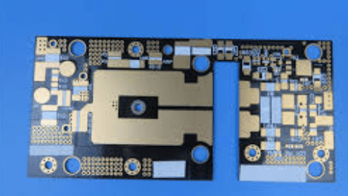
Upon receiving the fabricated PCB, the next phase is assembly.
This involves soldering the electronic components onto the board, either manually or using automated equipment such as pick-and-place machines and reflow ovens. For those new to soldering, it is recommended to practice on simpler projects before attempting more complex assemblies. Ensuring proper solder joints and verifying component placement can prevent issues such as short circuits or poor connections.
Finally, the assembled PCB must undergo testing to verify its functionality.
This can involve a range of techniques, from simple continuity checks with a multimeter to more advanced testing using oscilloscopes or logic analyzers. Identifying and addressing any issues at this stage is crucial, as it allows for further iterations and refinements of the design.
In conclusion, rapid PCB prototyping is a multi-step process that requires careful planning, attention to detail, and a methodical approach. By following this step-by-step guide, designers and engineers can efficiently develop and test their electronic circuits, ultimately leading to more successful and reliable products.
Common Mistakes To Avoid In PCB Prototyping
In the realm of electronics, quick PCB prototyping is a crucial step in the development process, allowing engineers and designers to test and refine their designs before mass production. However, despite its importance, there are several common mistakes that can hinder the effectiveness of PCB prototyping. By understanding and avoiding these pitfalls, one can ensure a smoother and more efficient prototyping process.
One of the most frequent errors in PCB prototyping is inadequate planning.
Often, designers rush into the prototyping phase without thoroughly considering the design requirements and constraints. This lack of foresight can lead to issues such as incorrect component placement, insufficient space for routing, and even design rule violations. To mitigate this, it is essential to invest time in detailed planning and schematic design, ensuring that all components are correctly specified and that the layout adheres to the necessary design rules.
Another prevalent mistake is neglecting to perform thorough design rule checks (DRCs).
DRCs are automated checks that verify whether a PCB layout complies with the predefined design rules. Skipping this step can result in a prototype that is not manufacturable or that exhibits performance issues. Therefore, it is crucial to run DRCs at various stages of the design process and address any violations promptly. This practice not only helps in identifying potential problems early but also saves time and resources in the long run.
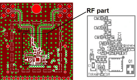
Furthermore, improper component selection can significantly impact the success of a PCB prototype.
Choosing components without considering their availability, lead times, and compatibility with the design can lead to delays and additional costs. It is advisable to select components that are readily available and have a stable supply chain. Additionally, verifying the compatibility of components with the design specifications and ensuring they meet the required performance criteria is vital.
In addition to component selection, another common mistake is overlooking thermal management.
PCBs can generate significant amounts of heat, especially in high-power applications. Failing to account for thermal dissipation can result in overheating, which can damage components and affect the overall performance of the prototype. To avoid this, designers should incorporate adequate thermal management strategies, such as using heat sinks, thermal vias, and proper component placement to ensure efficient heat dissipation.
Moreover, insufficient testing and validation of the prototype can lead to undetected issues that may only surface during later stages of development or even in the final product.
It is imperative to conduct comprehensive testing, including functional testing, signal integrity analysis, and thermal analysis, to validate the prototype’s performance under various conditions. This thorough testing helps in identifying and rectifying any issues early, thereby enhancing the reliability and robustness of the final design.
Lastly, poor documentation is a mistake that can complicate the prototyping process.
Clear and detailed documentation of the design, including schematics, layout files, and bill of materials (BOM), is essential for effective communication and collaboration among team members. Inadequate documentation can lead to misunderstandings, errors in manufacturing, and difficulties in troubleshooting. Therefore, maintaining meticulous documentation throughout the design and prototyping process is crucial.
In conclusion, quick PCB prototyping is an invaluable tool in the electronics development process, but it is fraught with potential pitfalls. By avoiding common mistakes such as inadequate planning, neglecting design rule checks, improper component selection, overlooking thermal management, insufficient testing, and poor documentation, designers can significantly enhance the efficiency and success of their prototyping efforts. Through careful attention to these aspects, one can ensure a smoother transition from prototype to final product, ultimately leading to a more reliable and high-quality outcome.
Top Software For Fast PCB Design And Prototyping
In the realm of electronics, the ability to swiftly design and prototype printed circuit boards (PCBs) is crucial for innovation and development. The process of PCB prototyping has been significantly streamlined by the advent of sophisticated software tools, which enable engineers and designers to create, test, and refine their designs with remarkable efficiency. Among the myriad of software options available, several stand out for their capabilities, user-friendliness, and comprehensive features.
One of the most prominent tools in the industry is Altium Designer.
Renowned for its powerful suite of features, Altium Designer offers an integrated environment that combines schematic capture, PCB layout, and design rule checking. This software is particularly favored for its advanced routing capabilities and extensive component libraries, which facilitate the rapid creation of complex designs. Moreover, Altium Designer’s real-time 3D visualization allows designers to inspect their boards in a virtual space, ensuring that all components fit correctly and that there are no unforeseen issues.
Transitioning to another notable software, Eagle by Autodesk is a popular choice among both hobbyists and professionals.
Eagle’s user-friendly interface and robust feature set make it an excellent tool for quick PCB prototyping. Its schematic editor and PCB layout editor are tightly integrated, allowing for seamless transitions between design stages. Additionally, Eagle’s extensive online community and library of pre-designed components provide valuable resources for designers looking to expedite their projects. The software’s affordability and scalability further enhance its appeal, making it accessible to a wide range of users.
KiCad, an open-source alternative, has gained significant traction in recent years due to its cost-free nature and powerful capabilities.
KiCad offers a comprehensive suite of tools for schematic capture, PCB layout, and 3D visualization. Its open-source model encourages community contributions, resulting in a constantly evolving platform with a wealth of user-generated libraries and plugins. This collaborative environment not only accelerates the design process but also fosters innovation and knowledge sharing among users. KiCad’s flexibility and extensive documentation make it a viable option for both beginners and seasoned professionals.
Another noteworthy mention is DipTrace, which is known for its intuitive interface and ease of use.
DipTrace provides a complete set of tools for schematic capture, PCB layout, and 3D modeling. Its component editor and pattern editor allow for the creation of custom components and footprints, catering to specific design requirements. DipTrace’s real-time design rule checking and error reporting ensure that potential issues are identified and resolved early in the design process, thereby reducing the likelihood of costly revisions. The software’s ability to import and export files in various formats also enhances its compatibility with other design tools and manufacturing processes.
In addition to these established tools, Upverter offers a cloud-based solution that facilitates collaborative PCB design.
Upverter’s online platform allows multiple users to work on a project simultaneously, streamlining the design process and enabling real-time feedback and iteration. This collaborative approach is particularly beneficial for teams working remotely or across different locations. Upverter’s integration with various component suppliers also simplifies the procurement process, ensuring that designers have access to the necessary parts for their prototypes.
In conclusion, the landscape of PCB design and prototyping software is rich with options that cater to different needs and preferences. Whether one prioritizes advanced features, user-friendliness, cost-effectiveness, or collaborative capabilities, there is a tool available to meet those requirements. By leveraging these powerful software solutions, designers can accelerate their development cycles, reduce errors, and bring innovative products to market more efficiently.