Quality control in pcb manufacturing
Importance Of Automated Optical Inspection In PCB Quality Control
In the realm of printed circuit board (PCB) manufacturing, quality control is paramount to ensure the reliability and functionality of the final product. One of the most critical components of this quality control process is Automated Optical Inspection (AOI). AOI systems play a crucial role in detecting defects and ensuring that PCBs meet stringent quality standards before they proceed to the next stage of production. The importance of AOI in PCB quality control cannot be overstated, as it significantly enhances the efficiency, accuracy, and overall quality of the manufacturing process.
To begin with, AOI systems utilize advanced imaging technology to inspect PCBs for a wide range of defects, including soldering issues, component misalignments, and surface irregularities.
By employing high-resolution cameras and sophisticated algorithms, AOI systems can quickly and accurately identify defects that might be missed by human inspectors. This level of precision is essential in the production of high-density and complex PCBs, where even the smallest defect can lead to significant performance issues or complete failure of the electronic device.
Moreover, the implementation of AOI in PCB manufacturing offers substantial time and cost savings.
Traditional manual inspection methods are not only time-consuming but also prone to human error. In contrast, AOI systems can inspect PCBs at a much faster rate, allowing manufacturers to maintain high production throughput without compromising on quality. This increased efficiency translates to reduced labor costs and shorter production cycles, ultimately leading to a more competitive market position for manufacturers.
In addition to speed and accuracy, AOI systems provide valuable data that can be used to improve the overall manufacturing process.
By analyzing the inspection results, manufacturers can identify recurring defects and pinpoint their root causes. This data-driven approach enables continuous improvement in production processes, leading to higher yields and reduced waste. Furthermore, the ability to track and document inspection results ensures that manufacturers can maintain compliance with industry standards and regulations, which is particularly important in sectors such as aerospace, automotive, and medical devices.
Another significant advantage of AOI is its ability to integrate seamlessly with other quality control and production systems.
Modern AOI systems can be easily incorporated into existing manufacturing lines, providing real-time feedback and enabling immediate corrective actions. This integration ensures that defects are detected and addressed at the earliest possible stage, preventing defective PCBs from advancing further in the production process. Consequently, this reduces the likelihood of costly rework or scrapping of defective boards, thereby enhancing overall production efficiency.
Furthermore, the versatility of AOI systems allows them to be used at various stages of the PCB manufacturing process.
From inspecting bare boards before component placement to verifying solder joints after reflow soldering, AOI systems provide comprehensive coverage throughout the production cycle. This multi-stage inspection capability ensures that defects are caught early and consistently, contributing to the production of high-quality PCBs.
In conclusion, the importance of Automated Optical Inspection in PCB quality control is evident in its ability to enhance accuracy, efficiency, and overall product quality. By leveraging advanced imaging technology and data analysis, AOI systems provide a reliable and cost-effective solution for detecting defects and ensuring compliance with industry standards. As PCB designs continue to evolve and become more complex, the role of AOI in maintaining high-quality manufacturing processes will only become more critical. Therefore, investing in AOI technology is not just a strategic decision but a necessity for manufacturers aiming to stay competitive in the ever-evolving electronics industry.
Best Practices For Ensuring PCB Reliability And Durability
Ensuring the reliability and durability of printed circuit boards (PCBs) is paramount in the electronics industry, where the performance and longevity of devices hinge on the quality of their internal components. To achieve this, manufacturers must adhere to a series of best practices in quality control throughout the PCB production process. These practices encompass meticulous attention to detail, rigorous testing, and adherence to industry standards, all of which contribute to the creation of robust and dependable PCBs.
One of the foundational steps in ensuring PCB reliability is the careful selection of materials.
High-quality substrates, copper foils, and solder masks are essential for creating a durable PCB. Manufacturers must source these materials from reputable suppliers and verify their compliance with industry standards such as IPC-4101 for base materials. By doing so, they can mitigate the risk of defects that could compromise the PCB’s performance.
In addition to material selection, the design phase plays a crucial role in the reliability of PCBs.
Engineers must employ design for manufacturability (DFM) principles to ensure that the PCB layout is optimized for production. This includes considerations such as trace width, spacing, and thermal management. By addressing potential issues at the design stage, manufacturers can prevent costly errors and rework during production.
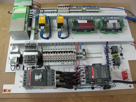
Once the design is finalized, the manufacturing process itself must be tightly controlled.
This begins with the fabrication of the PCB, where precision is key. Advanced techniques such as automated optical inspection (AOI) and X-ray inspection are employed to detect defects such as misaligned traces, insufficient solder, and voids. These inspections are critical for identifying issues early in the production process, allowing for timely corrective actions.
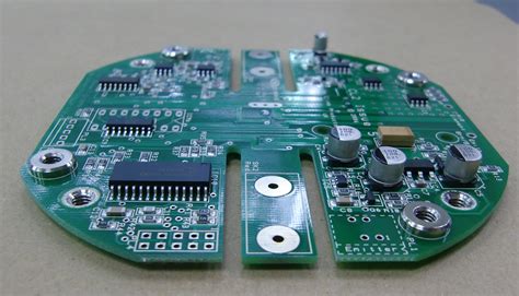
Following fabrication, the assembly process involves placing and soldering components onto the PCB.
Here, the use of automated equipment such as pick-and-place machines and reflow ovens ensures consistent and accurate component placement. However, human oversight remains essential, particularly for complex or high-reliability applications. Manual inspection and testing complement automated processes, providing an additional layer of quality assurance.
Testing is a cornerstone of quality control in PCB manufacturing.
Functional testing, in-circuit testing (ICT), and boundary scan testing are among the methods used to verify the performance of the assembled PCB. These tests help identify issues such as short circuits, open circuits, and component failures. By subjecting PCBs to rigorous testing, manufacturers can ensure that only fully functional boards proceed to the next stage of production.
Environmental testing is another critical aspect of ensuring PCB durability.
PCBs must withstand various environmental conditions, including temperature fluctuations, humidity, and mechanical stress. Accelerated life testing, thermal cycling, and vibration testing simulate these conditions to evaluate the PCB’s resilience. By exposing PCBs to harsh environments, manufacturers can identify potential weaknesses and make necessary improvements.
Finally, adherence to industry standards and certifications is essential for maintaining high-quality PCB production.
Standards such as IPC-A-610 for electronic assemblies and ISO 9001 for quality management systems provide guidelines for best practices in manufacturing. Compliance with these standards not only ensures product quality but also enhances customer confidence and satisfaction.
In conclusion, the reliability and durability of PCBs are the result of a comprehensive approach to quality control. From material selection and design optimization to precise manufacturing processes and rigorous testing, each step is crucial in producing high-quality PCBs. By adhering to best practices and industry standards, manufacturers can deliver reliable and durable PCBs that meet the demands of today’s advanced electronic devices.
Role Of X-Ray Inspection In Detecting PCB Defects
In the realm of printed circuit board (PCB) manufacturing, ensuring the highest quality is paramount. One of the most critical tools in achieving this objective is X-ray inspection. This advanced technology plays a pivotal role in detecting defects that could compromise the functionality and reliability of PCBs. As the complexity of electronic devices continues to escalate, the need for precise and thorough inspection methods becomes increasingly essential.
X-ray inspection, also known as automated X-ray inspection (AXI), is a non-destructive testing method that allows manufacturers to examine the internal structures of PCBs without causing any damage.
This capability is particularly valuable because many defects in PCBs are not visible to the naked eye or through traditional optical inspection methods. For instance, issues such as solder joint defects, component misalignments, and internal cracks can be effectively identified using X-ray technology.
One of the primary advantages of X-ray inspection is its ability to provide a detailed view of the internal layers of a PCB.
This is crucial because modern PCBs often consist of multiple layers, each with intricate circuitry and components. Traditional inspection methods may only reveal surface-level defects, leaving deeper issues undetected. X-ray inspection, however, penetrates through these layers, offering a comprehensive analysis of the entire board. Consequently, manufacturers can identify and address defects that might otherwise go unnoticed until the final product fails in the field.
Moreover, X-ray inspection is instrumental in detecting solder joint defects, which are among the most common issues in PCB manufacturing.
Solder joints are critical connections that ensure electrical continuity between components and the PCB. Defects such as voids, insufficient solder, and bridging can severely impact the performance of the final product. X-ray inspection allows for the precise evaluation of these joints, ensuring that they meet the required standards and specifications. By identifying and rectifying solder joint defects early in the manufacturing process, manufacturers can significantly reduce the risk of product failures and recalls.
In addition to solder joint inspection, X-ray technology is also effective in detecting component misalignments and placement errors.
As electronic devices become more compact, the components on PCBs are placed closer together, increasing the likelihood of misalignment. Even a slight deviation can lead to malfunctioning circuits and compromised performance. X-ray inspection provides a high-resolution image of the component placement, enabling manufacturers to verify that each component is correctly positioned. This level of precision is essential for maintaining the integrity and functionality of the final product.
Furthermore, X-ray inspection contributes to the overall efficiency of the PCB manufacturing process.
By identifying defects early, manufacturers can implement corrective actions before the boards proceed to subsequent stages of production. This proactive approach minimizes the need for rework and reduces production costs. Additionally, it enhances the overall yield, as fewer defective boards are produced. The ability to detect and address defects promptly ensures that only high-quality PCBs reach the market, thereby enhancing customer satisfaction and brand reputation.
In conclusion, X-ray inspection is an indispensable tool in the quality control of PCB manufacturing. Its ability to provide detailed insights into the internal structures of PCBs, detect solder joint defects, and verify component placement makes it a critical component of the manufacturing process. As electronic devices continue to evolve, the importance of X-ray inspection in ensuring the reliability and performance of PCBs cannot be overstated. By leveraging this advanced technology, manufacturers can uphold the highest standards of quality and deliver products that meet the stringent demands of today’s market.
Implementing Statistical Process Control In PCB Manufacturing
Implementing Statistical Process Control (SPC) in PCB manufacturing is a critical step towards ensuring the production of high-quality printed circuit boards. SPC is a method of quality control that employs statistical methods to monitor and control a process. By using SPC, manufacturers can identify variations in the production process that may lead to defects, thereby enabling them to take corrective actions before these variations result in faulty products. This proactive approach not only enhances the quality of the final product but also reduces waste and increases efficiency.
To begin with, the implementation of SPC in PCB manufacturing involves the collection and analysis of data from various stages of the production process.
This data is typically gathered through the use of control charts, which are graphical representations of a process over time. Control charts help in identifying trends, shifts, or any unusual patterns that may indicate a problem. By continuously monitoring these charts, manufacturers can detect deviations from the norm and address them promptly.
One of the primary benefits of using SPC in PCB manufacturing is the ability to maintain consistent quality.
Consistency is crucial in the electronics industry, where even minor defects can lead to significant issues in the final product. By identifying and correcting variations early in the process, manufacturers can ensure that each PCB meets the required specifications and performance standards. This not only enhances the reliability of the product but also builds trust with customers.
Moreover, SPC aids in reducing production costs. When defects are detected early, the cost of rework or scrap is significantly lower compared to identifying issues at the end of the production line.
This cost-saving aspect is particularly important in PCB manufacturing, where the complexity of the product can make rework both time-consuming and expensive. By minimizing waste and improving process efficiency, SPC contributes to a more cost-effective manufacturing process.
In addition to cost savings, SPC also plays a vital role in continuous improvement.
The data collected through SPC provides valuable insights into the production process, highlighting areas that may require improvement. By analyzing this data, manufacturers can implement changes that enhance the overall efficiency and quality of the process. This continuous feedback loop fosters a culture of ongoing improvement, which is essential in maintaining a competitive edge in the market.
Furthermore, the implementation of SPC in PCB manufacturing requires a commitment to training and education.
Employees at all levels must understand the principles of SPC and how to apply them effectively. This includes not only the technical aspects of data collection and analysis but also the importance of maintaining a quality-focused mindset. By investing in training, manufacturers can ensure that their workforce is equipped with the knowledge and skills necessary to support SPC initiatives.
In conclusion, implementing Statistical Process Control in PCB manufacturing is a strategic approach to achieving high-quality products and efficient production processes. By leveraging statistical methods to monitor and control the production process, manufacturers can identify and address variations early, ensuring consistent quality and reducing costs. Additionally, SPC fosters a culture of continuous improvement, driving ongoing enhancements in process efficiency and product reliability. Through a commitment to training and education, manufacturers can empower their workforce to effectively support SPC initiatives, ultimately leading to a more robust and competitive manufacturing operation.