Psa flex pcb
Advantages Of Using PSA Flex PCB In Modern Electronics
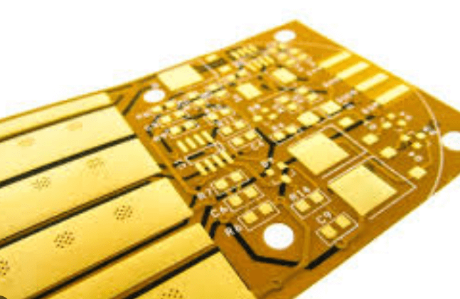
PSA Flex PCB, or Pressure-Sensitive Adhesive Flexible Printed Circuit Board, has emerged as a pivotal component in the realm of modern electronics. This innovative technology offers a multitude of advantages that cater to the evolving demands of contemporary electronic devices.
As the electronics industry continues to push the boundaries of miniaturization and functionality, PSA Flex PCB stands out as a solution that addresses several critical challenges.
One of the foremost advantages of PSA Flex PCB is its exceptional flexibility.
Unlike traditional rigid PCBs, PSA Flex PCBs can bend and conform to various shapes and surfaces. This flexibility is particularly beneficial in applications where space constraints and complex geometries are prevalent. For instance, in wearable technology, medical devices, and compact consumer electronics, the ability to integrate a flexible circuit board allows for more ergonomic and user-friendly designs. Consequently, manufacturers can create products that are not only more aesthetically pleasing but also more comfortable and practical for end-users.
In addition to flexibility, PSA Flex PCBs offer significant weight reduction.
The lightweight nature of these circuit boards is a crucial factor in industries such as aerospace and automotive, where every gram counts. By utilizing PSA Flex PCBs, manufacturers can achieve substantial weight savings, which in turn contributes to improved fuel efficiency and overall performance. This weight reduction does not come at the expense of durability; PSA Flex PCBs are designed to withstand mechanical stress and environmental factors, ensuring reliable performance even in demanding conditions.
Another notable advantage of PSA Flex PCB is its ease of installation.
The pressure-sensitive adhesive backing simplifies the assembly process, allowing for quick and secure attachment to various substrates. This adhesive property eliminates the need for additional fastening mechanisms, such as screws or clips, thereby streamlining the manufacturing process and reducing assembly time. Moreover, the adhesive provides excellent thermal and electrical insulation, enhancing the overall reliability and safety of the electronic device.
Furthermore, PSA Flex PCBs contribute to enhanced signal integrity.
The flexible nature of these circuit boards allows for shorter and more direct routing of electrical connections, minimizing signal loss and interference. This is particularly advantageous in high-frequency applications, where maintaining signal integrity is paramount. As a result, devices that incorporate PSA Flex PCBs can achieve superior performance and reliability, meeting the stringent requirements of modern electronic systems.
The environmental benefits of PSA Flex PCB should not be overlooked.
The materials used in these circuit boards are often more environmentally friendly compared to traditional rigid PCBs. Additionally, the reduced weight and compact design contribute to lower energy consumption during transportation and operation. This aligns with the growing emphasis on sustainability and eco-friendly practices within the electronics industry.
In conclusion, the advantages of using PSA Flex PCB in modern electronics are manifold. From exceptional flexibility and weight reduction to ease of installation and enhanced signal integrity, these circuit boards offer a comprehensive solution to the challenges faced by contemporary electronic devices. As technology continues to advance, the adoption of PSA Flex PCB is likely to become even more widespread, driving innovation and efficiency across various sectors. The integration of this technology not only enhances the performance and reliability of electronic devices but also supports the industry’s commitment to sustainability and environmental responsibility.
Design Considerations For PSA Flex PCB Applications
When designing PSA (Pressure-Sensitive Adhesive) flex PCBs, several critical considerations must be taken into account to ensure optimal performance and reliability. The unique properties of PSA flex PCBs, which combine the flexibility of traditional flexible circuits with the convenience of adhesive backing, make them suitable for a wide range of applications. However, their successful implementation hinges on meticulous design and material selection.
To begin with, the choice of materials is paramount.
The substrate material must be flexible yet durable, typically composed of polyimide or polyester films. These materials offer excellent thermal stability and mechanical strength, which are essential for maintaining the integrity of the circuit under various environmental conditions. Additionally, the adhesive layer must be carefully selected to provide strong bonding without compromising the flexibility of the PCB. Acrylic and silicone-based adhesives are commonly used due to their superior adhesion properties and resistance to temperature variations.
Another crucial aspect is the layout design.
The flexibility of PSA flex PCBs allows for innovative and compact designs, but it also necessitates careful planning to avoid mechanical stress and potential damage. Trace routing should be optimized to minimize bending stress, with wider traces and rounded corners preferred over sharp angles. This reduces the risk of trace cracking or delamination during flexing. Furthermore, the placement of components should be strategically planned to avoid areas of high mechanical stress, ensuring that critical components are not subjected to excessive bending or twisting.
Thermal management is another key consideration in the design of PSA flex PCBs.
The adhesive layer can act as an insulator, potentially trapping heat and affecting the performance of the circuit. Therefore, it is essential to incorporate effective thermal management strategies, such as the use of thermal vias, heat sinks, or conductive adhesives, to dissipate heat efficiently. This is particularly important in high-power applications where excessive heat generation could lead to circuit failure.
In addition to thermal management, electrical performance must be carefully evaluated.
The flexibility of the substrate can introduce variations in impedance, which can affect signal integrity, especially in high-frequency applications. To mitigate this, controlled impedance design techniques should be employed, ensuring consistent electrical performance across the entire flex PCB. This may involve precise control of trace width, spacing, and the dielectric properties of the substrate material.
Environmental factors also play a significant role in the design of PSA flex PCBs.
These circuits are often used in applications where they are exposed to harsh conditions, such as extreme temperatures, humidity, and chemical exposure. Therefore, the materials and adhesives used must be resistant to these environmental factors to ensure long-term reliability. Protective coatings, such as conformal coatings or encapsulants, can be applied to shield the circuit from moisture, dust, and other contaminants.
Finally, manufacturability and assembly processes must be considered.
The flexible nature of PSA flex PCBs can pose challenges during assembly, particularly in terms of handling and alignment. Automated assembly processes should be adapted to accommodate the unique properties of these circuits, ensuring precise placement and bonding of components. Additionally, testing and inspection procedures must be tailored to detect potential issues, such as delamination or trace damage, that could compromise the performance of the final product.
In conclusion, the design of PSA flex PCBs requires a comprehensive approach that addresses material selection, layout design, thermal management, electrical performance, environmental resistance, and manufacturability. By carefully considering these factors, designers can create robust and reliable PSA flex PCBs that meet the demands of a wide range of applications.
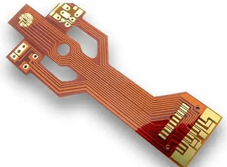
Manufacturing Process Of PSA Flex PCB: A Step-By-Step Guide
The manufacturing process of PSA (Pressure-Sensitive Adhesive) Flex PCBs (Printed Circuit Boards) is a meticulous and intricate procedure that demands precision and expertise. This process begins with the selection of appropriate materials, which is crucial for ensuring the final product’s reliability and performance. Typically, the base material used is a flexible polyimide film, chosen for its excellent thermal stability and mechanical properties. This film serves as the substrate upon which the circuit is built.
Once the substrate is prepared, the next step involves the application of a conductive layer, usually copper.
This is achieved through a process called lamination, where a thin copper foil is bonded to the polyimide film using heat and pressure. The lamination process must be carefully controlled to avoid any defects that could compromise the integrity of the circuit. Following lamination, the copper-clad substrate undergoes a cleaning process to remove any contaminants that might interfere with subsequent steps.
The cleaned substrate is then subjected to a photolithography process, which is essential for defining the circuit pattern.
Aphotoresist material is applied to the copper surface, and the desired circuit pattern is transferred onto the photoresist using ultraviolet (UV) light. The areas exposed to UV light harden, while the unexposed areas remain soft and can be washed away, revealing the underlying copper. This step is critical, as it determines the accuracy and precision of the circuit layout.
Subsequently, the exposed copper areas are etched away using a chemical solution, leaving behind the desired circuit pattern.
The etching process must be carefully monitored to ensure that the copper is removed uniformly, preventing any potential short circuits or open circuits. After etching, the remaining photoresist is stripped away, revealing the final copper circuit on the flexible substrate.
To enhance the durability and performance of the PSA Flex PCB, a protective layer, often referred to as a coverlay, is applied.
This coverlay is typically made of polyimide and serves to insulate and protect the copper traces from environmental factors such as moisture and mechanical stress. The coverlay is laminated onto the circuit using heat and pressure, similar to the initial lamination process.
Following the application of the coverlay, the PSA Flex PCB undergoes a series of inspections and tests to ensure its quality and functionality.
These inspections include visual checks for any physical defects, as well as electrical tests to verify the continuity and integrity of the circuit. Any defects identified during these inspections must be addressed and corrected to ensure the final product meets the required specifications.
The final step in the manufacturing process involves the application of the pressure-sensitive adhesive.
This adhesive layer is applied to the backside of the flexible PCB, allowing it to be easily mounted onto various surfaces without the need for additional fastening mechanisms. The adhesive must be carefully selected to ensure it provides a strong bond while maintaining the flexibility of the PCB.
In conclusion, the manufacturing process of PSA Flex PCBs is a complex and detailed procedure that requires careful attention to each step. From material selection and lamination to photolithography, etching, and the application of protective layers and adhesives, each stage plays a critical role in ensuring the final product’s performance and reliability. By adhering to stringent quality control measures and employing advanced manufacturing techniques, manufacturers can produce high-quality PSA Flex PCBs that meet the demands of various applications.
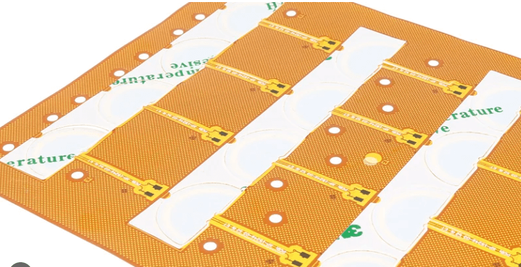
Common Challenges And Solutions In PSA Flex PCB Integration
Integrating PSA (Pressure-Sensitive Adhesive) Flex PCBs into electronic devices presents a unique set of challenges that engineers and designers must navigate to ensure optimal performance and reliability.
One of the primary challenges is the alignment and placement of the flex PCB.
Due to the flexible nature of these circuits, maintaining precise alignment during the assembly process can be difficult. Misalignment can lead to poor electrical connections and potential device failure. To address this, manufacturers often employ automated pick-and-place machines equipped with vision systems that can accurately position the flex PCB. Additionally, using alignment fixtures during manual assembly can help maintain the correct positioning.
Another significant challenge is ensuring the durability and longevity of the PSA flex PCB.
The adhesive used must provide a strong bond that can withstand various environmental conditions, such as temperature fluctuations, humidity, and mechanical stress. Selecting the appropriate adhesive is crucial; it must be compatible with the materials of both the flex PCB and the substrate to which it is being adhered. Engineers often conduct extensive testing to evaluate the performance of different adhesives under simulated operating conditions. This testing helps in identifying the most suitable adhesive that can maintain its bonding properties over the device’s expected lifespan.
Thermal management is also a critical concern in PSA flex PCB integration.
Flexible circuits are often used in compact devices where space is limited, leading to potential heat dissipation issues. Excessive heat can degrade the adhesive and the flex PCB itself, causing delamination or electrical failures. To mitigate this, designers may incorporate thermal vias, heat sinks, or thermal interface materials to enhance heat dissipation. Additionally, optimizing the layout of the flex PCB to minimize heat generation and improve airflow can significantly improve thermal management.
Electrical performance is another area where challenges arise.
The flexible nature of the PCB can introduce signal integrity issues, such as impedance mismatches and crosstalk, especially in high-frequency applications. Careful design considerations, such as controlled impedance traces and proper grounding techniques, are essential to maintain signal integrity. Simulation tools can be used during the design phase to predict and address potential electrical performance issues before the manufacturing stage.
Mechanical stress and strain are inherent challenges in applications involving flex PCBs, particularly in dynamic environments where the circuit may be subjected to repeated bending or flexing.
Over time, this can lead to fatigue and eventual failure of the conductive traces. To enhance the mechanical robustness of the flex PCB, designers can use strain relief features, such as curved traces and reinforced areas, to distribute stress more evenly. Additionally, selecting materials with higher flexural endurance can improve the overall durability of the flex PCB.
Finally, cost considerations play a significant role in the integration of PSA flex PCBs.
While the benefits of flexibility and space-saving are clear, the manufacturing process for flex PCBs can be more complex and expensive compared to rigid PCBs. To manage costs, it is essential to optimize the design for manufacturability, reducing unnecessary complexity and material usage. Collaborating closely with suppliers and manufacturers can also help identify cost-effective solutions without compromising on quality and performance.
In conclusion, integrating PSA flex PCBs into electronic devices involves addressing a range of challenges, from alignment and durability to thermal management and electrical performance. By employing precise assembly techniques, selecting appropriate materials, and optimizing design, engineers can overcome these challenges and leverage the advantages of flexible circuits in their applications.