Prototype pcb how to use
Step-By-Step Guide To Using Prototype PCBs For Beginners
Prototype PCBs, or printed circuit boards, are essential tools for electronics enthusiasts and professionals alike. They allow for the testing and validation of circuit designs before committing to mass production. For beginners, understanding how to use prototype PCBs can be a daunting task. However, by following a systematic approach, one can effectively utilize these boards to bring their electronic projects to life.
To begin with, it is crucial to have a clear circuit design in mind.
This design can be sketched on paper or created using electronic design automation (EDA) software. The design should include all the necessary components, such as resistors, capacitors, integrated circuits, and connectors, along with their respective connections. Once the design is finalized, the next step involves transferring this design onto the prototype PCB.
The first step in using a prototype PCB is to gather all the required components and tools.
This includes the prototype PCB itself, soldering iron, solder wire, flux, tweezers, wire cutters, and the electronic components specified in the design. It is also advisable to have a multimeter on hand for testing purposes. With all the materials ready, the process of assembling the circuit can commence.
Begin by placing the components on the prototype PCB according to the design layout.
It is important to ensure that each component is correctly oriented and positioned. For instance, polarized components like electrolytic capacitors and diodes must be placed with the correct polarity. Using tweezers can help in accurately positioning small components. Once all the components are in place, the next step is to solder them onto the PCB.
Soldering is a critical skill in PCB assembly.
To solder a component, heat the soldering iron and apply a small amount of solder to the tip. Then, place the tip of the soldering iron on the joint where the component lead meets the PCB pad. After a few seconds, feed solder wire into the joint until it flows and covers the pad and lead. Remove the soldering iron and allow the joint to cool. Repeat this process for all the components on the PCB. It is essential to ensure that each solder joint is clean and free of cold solder joints, which can lead to poor electrical connections.
After soldering all the components, it is prudent to inspect the PCB for any solder bridges or shorts.
Solder bridges occur when excess solder creates an unintended connection between two adjacent pads. These can be identified visually or by using a multimeter to check for continuity between pads that should not be connected. If any solder bridges are found, they can be removed using a desoldering pump or solder wick.
Once the inspection is complete, the next step is to test the assembled circuit.
Connect the power supply and use a multimeter to verify that the correct voltages are present at various points in the circuit. Additionally, check the functionality of the circuit by observing the expected behavior of the components. If any issues are detected, troubleshoot by checking the connections and ensuring that all components are functioning correctly.
In conclusion, using prototype PCBs involves a series of methodical steps, from designing the circuit to assembling and testing it. By carefully following these steps and paying attention to detail, beginners can successfully use prototype PCBs to develop and validate their electronic projects. This process not only helps in refining the design but also builds essential skills in electronics assembly and troubleshooting.
Essential Tools And Materials For Working With Prototype PCBs
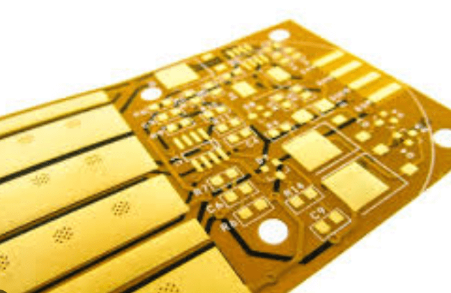
When embarking on the journey of working with prototype printed circuit boards (PCBs), it is crucial to be equipped with the essential tools and materials that will facilitate the process. The first and foremost requirement is the prototype PCB itself, which serves as the foundation for your electronic project. These boards are typically made from a non-conductive substrate, such as fiberglass, and are pre-patterned with conductive pathways to connect various electronic components.
To begin, a high-quality soldering iron is indispensable.
This tool allows you to securely attach components to the PCB by melting solder, a fusible metal alloy. It is advisable to use a soldering iron with adjustable temperature settings, as different components may require varying levels of heat. Alongside the soldering iron, solder wire is necessary. Lead-free solder is recommended for health and environmental reasons, although it may require a slightly higher temperature to melt.
In addition to the soldering iron and solder wire, a set of precision tweezers is essential for handling small components.
These tweezers enable you to place components accurately on the PCB, ensuring proper alignment and connection. Furthermore, a magnifying glass or a microscope can be extremely beneficial for inspecting your work, especially when dealing with miniature components and fine-pitch connections.
Another critical tool is the multimeter, which is used to measure electrical properties such as voltage, current, and resistance.
This device is invaluable for troubleshooting and verifying the functionality of your circuit. By using a multimeter, you can ensure that your connections are correct and that there are no short circuits or open circuits.
Wire cutters and strippers are also necessary for preparing and connecting wires to the PCB.
These tools allow you to cut wires to the desired length and strip the insulation from the ends, exposing the conductive core. This is particularly important when connecting external components or power sources to your prototype PCB.
A breadboard can be a useful addition to your toolkit, especially during the initial stages of prototyping.
This reusable platform allows you to build and test circuits without soldering, making it easier to make adjustments and modifications. Once you have a working prototype on the breadboard, you can then transfer the design to the PCB for a more permanent solution.
Flux is another material that can greatly enhance the soldering process.
This chemical agent helps to clean the surfaces being soldered, promoting better adhesion and reducing the likelihood of cold joints. Flux can be applied in various forms, including liquid, paste, or pen applicators, depending on your preference and the specific requirements of your project.
Lastly, having a good workspace is essential.
A well-lit, organized area with adequate ventilation will not only improve your efficiency but also ensure your safety. Proper ventilation is particularly important when soldering, as the fumes generated can be harmful if inhaled.
In conclusion, working with prototype PCBs requires a combination of specialized tools and materials to achieve successful results. By investing in high-quality equipment such as a soldering iron, precision tweezers, a multimeter, and wire cutters, you can ensure that your prototyping process is both efficient and effective. Additionally, utilizing materials like solder wire, flux, and a breadboard can further enhance your ability to create and test electronic circuits. With the right tools and a well-prepared workspace, you will be well-equipped to tackle any prototyping project with confidence and precision.
Common Mistakes To Avoid When Using Prototype PCBs
When working with prototype PCBs, it is crucial to be aware of common mistakes that can hinder the development process and lead to suboptimal results. One frequent error is neglecting to thoroughly check the design before sending it to fabrication. This oversight can result in costly revisions and delays. To avoid this, it is essential to meticulously review the schematic and layout, ensuring that all connections are correct and that there are no design rule violations. Utilizing design rule checks (DRC) and electrical rule checks (ERC) can help identify potential issues early in the design phase.
Another common mistake is underestimating the importance of proper component placement.
Poor placement can lead to signal integrity problems, increased electromagnetic interference (EMI), and difficulties in assembly. To mitigate these risks, it is advisable to place components logically, considering factors such as signal flow, power distribution, and thermal management. Grouping related components together and keeping high-speed signals short and direct can significantly improve the performance and reliability of the prototype PCB.
In addition to component placement, inadequate attention to trace routing can also cause significant issues.
Improperly routed traces can lead to crosstalk, impedance mismatches, and other signal integrity problems. To avoid these pitfalls, it is important to follow best practices for trace routing, such as maintaining consistent trace widths, using proper spacing between traces, and avoiding sharp angles. Additionally, employing techniques like differential pair routing and controlled impedance routing can help ensure signal integrity, especially in high-speed designs.
Power distribution is another critical aspect that is often overlooked.
Inadequate power distribution can result in voltage drops, noise, and instability in the circuit. To address this, it is essential to design a robust power distribution network (PDN) that provides clean and stable power to all components. This can be achieved by using wide power and ground planes, decoupling capacitors, and proper placement of power supply components. Ensuring that the PDN is well-designed can prevent many common power-related issues in prototype PCBs.
Thermal management is another area where mistakes are frequently made.
Overlooking the thermal requirements of components can lead to overheating and potential failure of the prototype PCB. To avoid this, it is important to consider the thermal characteristics of each component and design the PCB accordingly. This may involve adding thermal vias, heat sinks, or even redesigning the layout to improve airflow and heat dissipation. Proper thermal management ensures the longevity and reliability of the prototype PCB.
Furthermore, inadequate documentation can lead to confusion and errors during assembly and testing.
Providing clear and comprehensive documentation, including schematics, layout files, bill of materials (BOM), and assembly drawings, is essential for successful prototype PCB development. This documentation should be detailed enough to guide the assembly process and facilitate troubleshooting if issues arise.
Lastly, failing to test the prototype PCB thoroughly can result in undetected issues that may only surface later in the development process.
To avoid this, it is crucial to implement a rigorous testing regimen, including functional testing, signal integrity testing, and thermal testing. Identifying and addressing issues early in the prototype stage can save time and resources in the long run.
In conclusion, by being aware of and avoiding these common mistakes, engineers can significantly improve the success rate of their prototype PCB projects. Thorough design reviews, proper component placement, careful trace routing, robust power distribution, effective thermal management, comprehensive documentation, and rigorous testing are all essential practices that contribute to the development of reliable and high-performing prototype PCBs.
Advanced Techniques For Efficient Prototype PCB Usage
Prototype PCBs (Printed Circuit Boards) are essential tools in the development and testing of electronic circuits. They allow engineers and designers to experiment with circuit designs before committing to mass production. To maximize the efficiency and effectiveness of prototype PCB usage, it is crucial to employ advanced techniques that streamline the process and enhance the reliability of the final product.
One of the first steps in using prototype PCBs efficiently is to ensure meticulous planning and design.
Utilizing advanced software tools for PCB design, such as Altium Designer or Eagle, can significantly improve the accuracy and functionality of the prototype. These tools offer features like real-time error checking, component libraries, and simulation capabilities, which help in identifying potential issues early in the design phase. By addressing these issues beforehand, one can avoid costly and time-consuming revisions later in the process.
Transitioning from design to fabrication, it is essential to select the appropriate materials and manufacturing techniques.
High-quality substrates, such as FR4 or Rogers materials, provide better performance and durability. Additionally, opting for advanced fabrication methods like multi-layer PCBs or HDI (High-Density Interconnect) technology can enhance the prototype’s capabilities, especially for complex and high-speed circuits. These techniques allow for more compact designs and improved signal integrity, which are critical for modern electronic applications.
Once the prototype PCB is fabricated, the next step is assembly.
Employing surface-mount technology (SMT) rather than through-hole components can lead to more efficient and reliable assemblies. SMT components are smaller and can be placed on both sides of the PCB, allowing for more compact and intricate designs. Automated pick-and-place machines can further streamline the assembly process, ensuring precise component placement and reducing the likelihood of human error.
Testing and validation are crucial stages in the prototype PCB process.
Advanced testing techniques, such as Automated Optical Inspection (AOI) and X-ray inspection, can detect defects that are not visible to the naked eye. These methods provide a higher level of assurance that the prototype is free from manufacturing defects. Additionally, employing in-circuit testing (ICT) and functional testing can verify that the circuit operates as intended. These tests help identify any issues related to component functionality or circuit design, allowing for timely corrections.
To further enhance the efficiency of prototype PCB usage, it is beneficial to adopt a modular approach to design.
By creating reusable modules or building blocks for common circuit functions, one can quickly assemble and test new designs without starting from scratch. This approach not only saves time but also improves the reliability of the prototypes, as the modules have been previously tested and validated.
Documentation is another critical aspect of efficient prototype PCB usage.
Maintaining detailed records of the design, fabrication, assembly, and testing processes ensures that any issues can be traced and addressed promptly. Comprehensive documentation also facilitates communication among team members and provides a valuable reference for future projects.
In conclusion, employing advanced techniques for prototype PCB usage can significantly enhance the efficiency and reliability of the development process. Meticulous planning and design, selecting appropriate materials and manufacturing methods, utilizing modern assembly techniques, and conducting thorough testing and validation are all essential steps. Additionally, adopting a modular design approach and maintaining detailed documentation can further streamline the process. By integrating these advanced techniques, engineers and designers can ensure that their prototype PCBs meet the highest standards of performance and reliability, ultimately leading to successful product development.