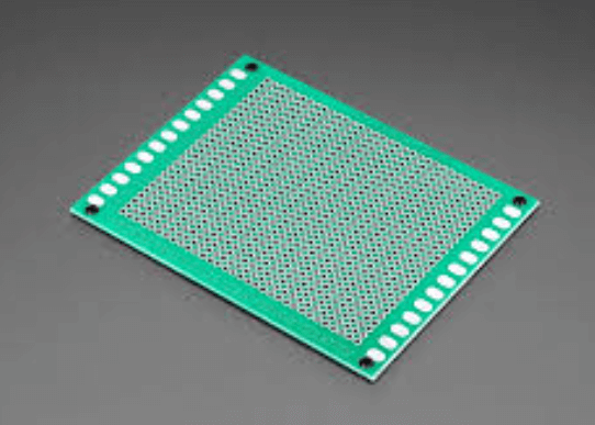
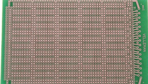
Prototype pcb 2mm pitch
Advantages Of Using 2mm Pitch In Prototype PCBs
The use of 2mm pitch in prototype printed circuit boards (PCBs) offers several advantages that can significantly enhance the design and functionality of electronic devices.
One of the primary benefits is the increased density of components that can be achieved.
With a 2mm pitch, designers can place components closer together, which is particularly advantageous in applications where space is at a premium. This compact arrangement not only saves valuable real estate on the PCB but also allows for more complex circuitry to be implemented within a smaller footprint.
Moreover, the 2mm pitch facilitates improved signal integrity.
When components are placed closer together, the length of the traces connecting them is reduced. Shorter traces are less susceptible to signal degradation and electromagnetic interference (EMI), which can be critical in high-speed or high-frequency applications. Consequently, the overall performance and reliability of the electronic device are enhanced, making the 2mm pitch an attractive option for advanced prototype PCBs.
In addition to signal integrity, thermal management is another area where the 2mm pitch offers significant advantages.
The compact layout allows for more efficient heat dissipation, as the proximity of components can facilitate better thermal conduction paths. This is particularly important in high-power applications where effective thermal management is crucial to prevent overheating and ensure the longevity of the components. By optimizing the thermal performance, the 2mm pitch contributes to the overall durability and reliability of the prototype PCB.
Furthermore, the 2mm pitch can lead to cost savings in the manufacturing process.
The reduced size of the PCB can lower material costs, as less substrate material is required. Additionally, the smaller footprint can result in more efficient use of manufacturing equipment, potentially increasing production throughput and reducing labor costs. These economic benefits make the 2mm pitch an appealing choice for both small-scale prototyping and large-scale production runs.
Another advantage of using a 2mm pitch in prototype PCBs is the potential for enhanced mechanical stability.
The closer spacing of components can provide a more robust structure, reducing the likelihood of mechanical failure due to vibration or physical stress. This is particularly beneficial in applications where the PCB may be subjected to harsh environmental conditions or mechanical shocks. The increased mechanical stability ensures that the prototype PCB can withstand the rigors of real-world use, thereby improving its overall reliability.
Moreover, the 2mm pitch can simplify the design process by providing a standardized spacing that is compatible with a wide range of components and connectors.
This standardization can streamline the design and assembly process, reducing the likelihood of errors and improving the overall efficiency of the development cycle. By facilitating a more straightforward design process, the 2mm pitch allows engineers to focus on optimizing the functionality and performance of the prototype PCB.
In conclusion, the use of a 2mm pitch in prototype PCBs offers numerous advantages, including increased component density, improved signal integrity, enhanced thermal management, cost savings, mechanical stability, and simplified design processes. These benefits make the 2mm pitch an attractive option for a wide range of applications, from high-speed electronics to high-power devices. By leveraging the advantages of the 2mm pitch, designers can create more compact, reliable, and cost-effective prototype PCBs that meet the demands of modern electronic devices.
Design Tips For Prototype PCBs With 2mm Pitch
When designing prototype PCBs with a 2mm pitch, it is essential to consider several critical factors to ensure the functionality and reliability of the final product. The 2mm pitch, which refers to the distance between the centers of adjacent pins or pads, presents unique challenges and opportunities that must be addressed during the design phase. By adhering to best practices and leveraging advanced design tools, engineers can optimize their PCB layouts for performance and manufacturability.
To begin with, understanding the implications of a 2mm pitch is crucial.
This pitch size is relatively larger compared to more common pitches like 1.27mm or 0.8mm, which can simplify certain aspects of the design process. For instance, the larger pitch allows for more straightforward routing of traces and can reduce the risk of short circuits and crosstalk between adjacent pins. However, it also means that the overall size of the PCB may increase, which could be a limiting factor in applications where space is at a premium.
One of the primary considerations when working with a 2mm pitch is the selection of appropriate components.
It is vital to choose components that are compatible with the 2mm pitch to avoid alignment issues during assembly. Additionally, ensuring that the components are readily available and not subject to long lead times can help prevent delays in the prototyping process. Engineers should also pay attention to the thermal characteristics of the components, as larger pitch sizes can affect heat dissipation and thermal management.
Another important aspect is the layout of the PCB.
Effective layout design can significantly impact the performance and reliability of the prototype. When designing the layout, it is advisable to maintain a consistent grid system that aligns with the 2mm pitch. This approach can simplify the routing process and help avoid potential alignment issues. Furthermore, using a grid system can facilitate the placement of vias and other interconnects, ensuring that they are optimally positioned to support signal integrity and power distribution.
Signal integrity is another critical factor to consider.
The 2mm pitch can influence the electrical characteristics of the PCB, including impedance and signal propagation. To mitigate potential issues, engineers should carefully design the trace widths and spacing to match the desired impedance. Additionally, incorporating ground planes and proper shielding techniques can help minimize electromagnetic interference (EMI) and ensure clean signal transmission.
Thermal management is also a key consideration in the design of prototype PCBs with a 2mm pitch.
The larger pitch size can impact the thermal performance of the PCB, as it may affect the distribution of heat across the board. To address this, engineers should incorporate thermal vias and heat sinks where necessary to enhance heat dissipation. Additionally, selecting materials with good thermal conductivity can help manage heat more effectively.
Finally, manufacturability should always be a priority in the design process.
Ensuring that the PCB design adheres to standard manufacturing practices can help avoid potential issues during production. This includes verifying that the design meets the tolerances and capabilities of the chosen fabrication and assembly processes. By collaborating closely with manufacturers and leveraging their expertise, engineers can optimize their designs for efficient and cost-effective production.
In conclusion, designing prototype PCBs with a 2mm pitch requires careful consideration of various factors, including component selection, layout design, signal integrity, thermal management, and manufacturability. By following best practices and leveraging advanced design tools, engineers can create reliable and high-performance PCBs that meet the specific requirements of their applications.
Common Applications For 2mm Pitch Prototype PCBs
Prototype PCBs with a 2mm pitch are increasingly becoming a staple in various technological applications due to their unique advantages and versatility. These printed circuit boards, characterized by the 2mm spacing between the centers of adjacent pins or pads, offer a balance between compactness and ease of handling, making them suitable for a wide range of uses. Understanding the common applications for 2mm pitch prototype PCBs can provide insight into their growing popularity and the reasons behind their selection in different technological domains.
One of the primary applications for 2mm pitch prototype PCBs is in the development of consumer electronics.
Devices such as smartphones, tablets, and wearable technology often require compact and efficient circuit designs. The 2mm pitch allows for a denser arrangement of components without compromising the ease of assembly and testing. This balance is crucial in consumer electronics, where space is at a premium, and reliability is paramount. Moreover, the ability to prototype with 2mm pitch PCBs enables designers to iterate quickly and refine their designs before moving to mass production.
In addition to consumer electronics, 2mm pitch prototype PCBs are widely used in the automotive industry.
Modern vehicles are equipped with numerous electronic systems, including advanced driver-assistance systems (ADAS), infotainment systems, and various sensors. These systems demand robust and reliable PCBs that can withstand harsh environmental conditions such as temperature fluctuations and vibrations. The 2mm pitch provides a suitable compromise between component density and mechanical stability, ensuring that the PCBs can perform reliably over the vehicle’s lifespan. Furthermore, the prototyping phase is critical in the automotive industry to ensure that all electronic systems function correctly and safely before full-scale production.
The medical field also benefits significantly from the use of 2mm pitch prototype PCBs.
Medical devices, ranging from diagnostic equipment to wearable health monitors, require precise and reliable electronic components. The 2mm pitch allows for the integration of complex circuits in a compact form factor, which is essential for portable and wearable medical devices. Additionally, the prototyping process is vital in the medical industry to ensure that devices meet stringent regulatory standards and perform accurately in clinical settings. The ability to quickly prototype and test with 2mm pitch PCBs accelerates the development process and helps bring innovative medical solutions to market faster.
Another notable application of 2mm pitch prototype PCBs is in the field of industrial automation.
Factories and production lines increasingly rely on sophisticated electronic systems to control machinery, monitor processes, and ensure safety. These systems often require custom PCBs that can handle high power loads and operate reliably in demanding environments. The 2mm pitch provides the necessary balance between component density and durability, making it an ideal choice for industrial applications. Prototyping with 2mm pitch PCBs allows engineers to develop and test custom solutions tailored to specific industrial needs, ensuring optimal performance and reliability.
In conclusion, the versatility and advantages of 2mm pitch prototype PCBs make them suitable for a wide range of applications, including consumer electronics, automotive systems, medical devices, and industrial automation. Their ability to balance compactness with ease of handling, combined with the critical role of prototyping in these industries, underscores their growing importance in modern technology development. As technological advancements continue to evolve, the demand for efficient and reliable prototype PCBs with a 2mm pitch is likely to increase, further solidifying their role in various high-tech applications.
Challenges And Solutions In Manufacturing 2mm Pitch Prototype PCBs
Manufacturing prototype PCBs with a 2mm pitch presents a unique set of challenges that require meticulous attention to detail and advanced technological solutions. The 2mm pitch, referring to the distance between the centers of adjacent pins or pads, demands precision in both design and production processes.
One of the primary challenges in this context is ensuring the accuracy of the layout.
Given the reduced spacing, even minor deviations can lead to significant issues such as short circuits or signal interference. To address this, manufacturers often employ high-resolution design software that allows for precise placement and routing of components.
Another significant challenge is the fabrication process itself.
The smaller pitch necessitates the use of advanced photolithography techniques to accurately transfer the design onto the PCB substrate. Traditional methods may not provide the required resolution, leading to defects that can compromise the functionality of the prototype. To mitigate this, manufacturers have turned to laser direct imaging (LDI) technology, which offers higher precision and better control over the etching process. This ensures that the intricate patterns required for a 2mm pitch are faithfully reproduced on the PCB.
In addition to layout and fabrication, the assembly of components on a 2mm pitch PCB poses its own set of difficulties.
The reduced spacing between pads means that there is less margin for error when placing and soldering components. Automated pick-and-place machines, equipped with high-precision vision systems, are often used to ensure accurate component placement. Furthermore, advanced soldering techniques such as reflow soldering are employed to achieve reliable connections without causing thermal damage to the components or the PCB itself.
Quality control is another critical aspect that cannot be overlooked.
Given the complexity and precision required for 2mm pitch PCBs, thorough inspection and testing are essential to identify and rectify any defects. Automated optical inspection (AOI) systems are commonly used to examine the PCBs for any visual defects such as misaligned components or solder bridges. Additionally, electrical testing methods such as flying probe testing are employed to verify the functionality of the circuits. These tests help ensure that the prototype meets the required specifications and performs as intended.
Despite these challenges, advancements in technology have provided effective solutions that enable the successful manufacturing of 2mm pitch prototype PCBs.
The integration of computer-aided design (CAD) tools with manufacturing processes has streamlined the transition from design to production, reducing the likelihood of errors. Moreover, the use of high-precision equipment and automated systems has significantly improved the accuracy and reliability of the final product.
In conclusion, while the manufacturing of 2mm pitch prototype PCBs presents several challenges, the adoption of advanced technologies and meticulous quality control measures have made it possible to overcome these obstacles. The precision required in design, fabrication, assembly, and inspection necessitates a comprehensive approach that leverages the latest advancements in the field. By doing so, manufacturers can ensure the production of high-quality prototype PCBs that meet the stringent requirements of modern electronic applications.