Printing flexible pcb
Advantages Of Printing Flexible PCBs For Modern Electronics
Printing flexible PCBs (Printed Circuit Boards) has emerged as a transformative technology in the realm of modern electronics, offering a multitude of advantages that cater to the evolving demands of contemporary devices.
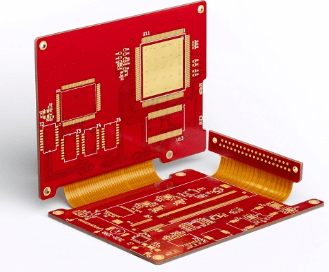
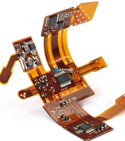
One of the primary benefits of flexible PCBs is their ability to conform to various shapes and contours,
which is particularly advantageous in the design of compact and intricate electronic devices. This flexibility allows for innovative product designs that were previously unattainable with traditional rigid PCBs, thereby enabling the development of more ergonomic and space-efficient gadgets.
Moreover, the lightweight nature of flexible PCBs significantly contributes to the reduction of the overall weight of electronic devices.
This is especially critical in applications such as wearable technology, medical devices, and aerospace electronics, where minimizing weight is paramount. The thin and light characteristics of flexible PCBs do not compromise their functionality, making them an ideal choice for these specialized applications.
In addition to their physical adaptability, flexible PCBs offer enhanced durability and reliability.
The materials used in their construction, such as polyimide or polyester films, provide excellent resistance to environmental stressors, including extreme temperatures, moisture, and chemicals. This resilience ensures that flexible PCBs maintain their performance and integrity even in harsh operating conditions, thereby extending the lifespan of the electronic devices in which they are used.
Another significant advantage of printing flexible PCBs is the potential for cost savings in both manufacturing and assembly processes.
The ability to print circuits directly onto flexible substrates reduces the need for multiple interconnects and connectors, which can be both costly and time-consuming to install. This streamlined approach not only lowers production costs but also enhances the overall reliability of the electronic device by reducing potential points of failure.
Furthermore, the integration of flexible PCBs into modern electronics facilitates improved signal integrity and electrical performance.
The close proximity of components on a flexible PCB minimizes the length of interconnections, thereby reducing signal loss and electromagnetic interference. This is particularly beneficial in high-frequency applications where maintaining signal integrity is crucial for optimal performance.
The versatility of flexible PCBs also extends to their compatibility with a wide range of electronic components and technologies.
They can be seamlessly integrated with rigid PCBs to create rigid-flex circuits, which combine the best attributes of both types of boards. This hybrid approach allows for greater design flexibility and can accommodate complex electronic systems that require both rigid and flexible elements.
In the context of sustainability, flexible PCBs contribute to the reduction of electronic waste.
Their durability and long lifespan mean that devices incorporating flexible PCBs are less likely to require frequent replacements. Additionally, the materials used in flexible PCBs are often more environmentally friendly compared to those used in traditional rigid PCBs, further supporting eco-friendly manufacturing practices.
In conclusion, the advantages of printing flexible PCBs for modern electronics are manifold, encompassing design flexibility, weight reduction, durability, cost efficiency, improved performance, and environmental sustainability. As the demand for more sophisticated and compact electronic devices continues to grow, the adoption of flexible PCBs is poised to play a pivotal role in shaping the future of electronic design and manufacturing.
Step-By-Step Guide To Printing Flexible PCBs At Home
Printing flexible PCBs at home can be a rewarding endeavor for electronics enthusiasts and professionals alike. The process, while intricate, is manageable with the right tools and a methodical approach. To begin, it is essential to gather all necessary materials, including a flexible copper-clad laminate, a laser printer, glossy paper, ferric chloride solution, a laminator or iron, and protective gear such as gloves and goggles.
The first step involves designing the PCB layout using specialized software like Eagle, KiCad, or Altium Designer
These programs allow for precise control over the circuit design, ensuring that all components are correctly placed and connected. Once the design is complete, it should be printed onto glossy paper using a laser printer. The toner from the laser printer will later serve as a resist during the etching process.
Next, prepare the flexible copper-clad laminate by cutting it to the desired size.
It is crucial to clean the surface of the laminate thoroughly to remove any oils or contaminants that could interfere with the transfer process. This can be done using isopropyl alcohol and a lint-free cloth. Once the laminate is clean, align the printed design with the copper side of the laminate.
The transfer process involves using heat to bond the toner from the glossy paper to the copper surface.
A laminator is ideal for this purpose, as it provides consistent heat and pressure. However, an iron can also be used if a laminator is not available. Carefully place the laminate and printed design into the laminator or press the iron onto the paper, applying even pressure and heat. This step requires patience, as insufficient heat or pressure can result in an incomplete transfer.
After the transfer is complete, allow the laminate to cool before carefully peeling away the glossy paper.
The toner should remain on the copper surface, forming a resist pattern that matches the original design. Inspect the transfer for any gaps or imperfections, as these can affect the final PCB. If necessary, use a permanent marker to touch up any areas where the toner did not adhere properly.
The next phase is etching, which removes the exposed copper, leaving only the areas protected by the toner.
Ferric chloride is a commonly used etchant for this purpose. Prepare a solution of ferric chloride in a plastic container, following the manufacturer’s instructions for concentration and safety precautions. Submerge the laminate in the solution, agitating it gently to ensure even exposure. The etching process can take anywhere from a few minutes to an hour, depending on the concentration of the solution and the thickness of the copper.
Once the unwanted copper has been etched away, remove the laminate from the solution and rinse it thoroughly with water to stop the etching process.
The remaining toner can be removed using acetone or isopropyl alcohol, revealing the final copper traces of the PCB. Inspect the board for any defects or incomplete etching, and use a multimeter to check for continuity between the traces.
Finally, drill any necessary holes for component leads using a precision drill. This step requires a steady hand and careful attention to the design specifications. Once the holes are drilled, the flexible PCB is ready for component placement and soldering.
By following these steps meticulously, one can successfully print flexible PCBs at home, enabling the creation of custom electronic projects with professional-quality results.
Common Challenges In Printing Flexible PCBs And How To Overcome Them
Printing flexible PCBs (Printed Circuit Boards) presents a unique set of challenges that differ significantly from those encountered with traditional rigid PCBs. These challenges stem from the inherent properties of the flexible materials used, as well as the specific requirements of the applications they serve. Understanding these challenges and implementing effective strategies to overcome them is crucial for ensuring the reliability and performance of flexible PCBs.
One of the primary challenges in printing flexible PCBs is the material selection.
Flexible PCBs are typically made from polyimide or polyester films, which offer the necessary flexibility but also introduce complexities in the manufacturing process. These materials can be more difficult to handle and process compared to the rigid substrates used in traditional PCBs. To address this, manufacturers must ensure that their equipment and processes are specifically designed to accommodate the unique properties of flexible materials. This includes using specialized printers and handling techniques that minimize the risk of damage or deformation during production.
Another significant challenge is maintaining dimensional stability throughout the printing process.
Flexible materials are prone to stretching and warping, which can lead to misalignment of the printed circuitry. This issue can be mitigated by carefully controlling the tension and temperature during the printing process. Additionally, using fiducial marks and alignment systems can help ensure that the printed patterns remain accurate and consistent, even when the substrate undergoes slight movements or deformations.
The adhesion of conductive inks to flexible substrates is also a critical concern.
Unlike rigid PCBs, where the copper layer is firmly bonded to the substrate, flexible PCBs rely on conductive inks that must adhere well to the flexible material. Poor adhesion can result in delamination or cracking of the conductive traces, leading to circuit failures. To enhance adhesion, surface treatments such as plasma cleaning or chemical etching can be employed to improve the bonding properties of the substrate. Furthermore, selecting inks that are specifically formulated for flexible applications can provide better adhesion and durability.
Thermal management is another area where flexible PCBs pose unique challenges.
The thin and flexible nature of these substrates means they have lower thermal mass and can be more susceptible to heat-related issues. Excessive heat during the printing or soldering processes can cause warping or damage to the flexible material. To overcome this, manufacturers must carefully control the thermal profiles during production and consider using low-temperature soldering techniques. Additionally, incorporating thermal vias or heat spreaders into the design can help dissipate heat more effectively and prevent localized hotspots.
Finally, ensuring the mechanical reliability of flexible PCBs is essential, especially in applications where they will be subjected to repeated bending or flexing.
The design of the PCB must account for the mechanical stresses it will encounter in its intended application. This can involve optimizing the layout to distribute stress more evenly, using strain relief features, and selecting materials that offer a good balance of flexibility and durability. Rigorous testing, including flexural fatigue testing, can help identify potential failure points and ensure that the final product meets the required reliability standards.
In conclusion, while printing flexible PCBs presents several challenges, these can be effectively managed through careful material selection, process control, and design optimization. By addressing issues related to material handling, dimensional stability, adhesion, thermal management, and mechanical reliability, manufacturers can produce high-quality flexible PCBs that meet the demanding requirements of modern electronic applications.
Innovations In Printing Flexible PCBs: What To Expect In The Future
The field of flexible printed circuit boards (PCBs) has seen remarkable advancements in recent years, driven by the increasing demand for more compact, lightweight, and versatile electronic devices. As technology continues to evolve, the innovations in printing flexible PCBs are poised to revolutionize various industries, from consumer electronics to medical devices and beyond. Understanding these advancements and what to expect in the future is crucial for stakeholders looking to stay ahead in this rapidly changing landscape.
One of the most significant innovations in the realm of flexible PCBs is the development of advanced materials.
Traditional rigid PCBs are typically made from fiberglass-reinforced epoxy, which, while durable, lacks the flexibility required for modern applications. In contrast, flexible PCBs are constructed from materials such as polyimide or polyester, which offer the necessary pliability. Recent research has focused on enhancing these materials to improve their thermal stability, electrical performance, and mechanical strength. For instance, the incorporation of nanomaterials like graphene and carbon nanotubes has shown promise in boosting the conductivity and durability of flexible PCBs, paving the way for more robust and efficient designs.
In addition to material advancements, the methods used to print flexible PCBs have also seen significant improvements.
Traditional photolithography techniques, while effective, are often time-consuming and costly. Emerging printing technologies, such as inkjet and screen printing, offer a more efficient and cost-effective alternative. These methods allow for the precise deposition of conductive inks onto flexible substrates, enabling the production of intricate circuit patterns with minimal waste. Moreover, additive manufacturing techniques, such as 3D printing, are beginning to make their mark in the industry. By building circuits layer by layer, 3D printing offers unparalleled design flexibility and the potential for rapid prototyping, which can significantly shorten development cycles.
As we look to the future, the integration of flexible PCBs with other emerging technologies holds immense potential.
One such area is the Internet of Things (IoT), where flexible PCBs can be used to create compact, lightweight sensors and devices that can be embedded in various environments. This integration can lead to the development of smart textiles, wearable health monitors, and other innovative applications that require seamless connectivity and real-time data collection. Furthermore, the advent of flexible displays and foldable smartphones has already begun to showcase the possibilities of flexible PCBs in consumer electronics, hinting at a future where devices are not only more functional but also more aesthetically pleasing.
Another promising avenue is the use of flexible PCBs in medical devices.
The biocompatibility and flexibility of these circuits make them ideal for applications such as implantable sensors, wearable health monitors, and even electronic skin. These devices can provide continuous monitoring of vital signs, offering valuable data for both patients and healthcare providers. As the technology matures, we can expect to see more sophisticated medical devices that leverage the unique properties of flexible PCBs to improve patient outcomes and enhance the overall quality of care.
In conclusion, the innovations in printing flexible PCBs are set to transform a wide range of industries by enabling the creation of more versatile, efficient, and compact electronic devices. Advances in materials, printing techniques, and integration with other technologies are driving this evolution, opening up new possibilities for applications that were once considered unattainable. As we move forward, staying abreast of these developments will be essential for those looking to capitalize on the opportunities presented by this dynamic and rapidly advancing field.