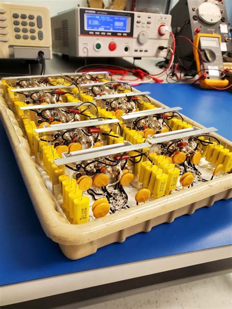
Printed wiring board assembly
Advances In Printed Wiring Board Assembly Techniques
Printed wiring board (PWB) assembly has undergone significant advancements in recent years, driven by the increasing complexity and miniaturization of electronic devices. These advancements have been pivotal in meeting the demands for higher performance, reliability, and efficiency in various applications, ranging from consumer electronics to aerospace systems.
One of the most notable developments in PWB assembly techniques is the adoption of surface mount technology (SMT).
SMT has largely replaced through-hole technology due to its ability to accommodate smaller components and higher component densities. This shift has enabled manufacturers to produce more compact and lightweight electronic devices without compromising functionality.
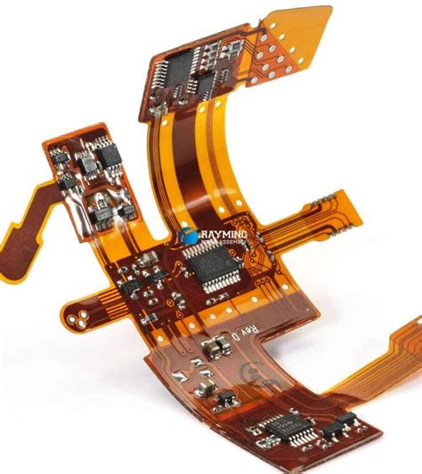
In addition to SMT, the use of advanced materials has also played a crucial role in enhancing PWB assembly.
High-performance substrates, such as polyimide and ceramic-based materials, offer superior thermal stability and electrical insulation properties. These materials are particularly beneficial in high-frequency and high-power applications, where traditional FR-4 substrates may fall short. Furthermore, the integration of flexible and rigid-flex PWBs has opened new possibilities for innovative product designs, allowing for greater versatility and durability in electronic assemblies.
Another significant advancement in PWB assembly is the implementation of automated assembly processes.
Automation has revolutionized the industry by improving precision, reducing human error, and increasing production throughput. Automated pick-and-place machines, for instance, can accurately position thousands of components per hour, significantly speeding up the assembly process. Additionally, automated optical inspection (AOI) systems have become indispensable in ensuring the quality and reliability of assembled PWBs. These systems use advanced imaging and machine learning algorithms to detect defects and inconsistencies, thereby minimizing the risk of faulty products reaching the market.
The advent of advanced soldering techniques has further contributed to the progress in PWB assembly.
Reflow soldering, which involves melting solder paste to create electrical connections, has become the standard method for attaching surface-mounted components. Innovations in reflow soldering, such as the use of nitrogen atmospheres and vapor phase soldering, have improved solder joint quality and reduced the occurrence of defects like voids and tombstoning. Moreover, selective soldering techniques have been developed to address the challenges of soldering through-hole components on mixed-technology boards, ensuring reliable connections without damaging sensitive SMT components.
In parallel with these technological advancements, the industry has also seen improvements in design and simulation tools.
Modern computer-aided design (CAD) software allows engineers to create highly detailed and accurate PWB layouts, optimizing component placement and routing for better performance and manufacturability. Simulation tools, on the other hand, enable the analysis of thermal, electrical, and mechanical properties of the PWB assembly, helping to identify potential issues before the manufacturing stage. These tools have become essential in the design process, reducing the time and cost associated with prototyping and testing.
Environmental considerations have also influenced advancements in PWB assembly techniques.
The push for lead-free soldering, driven by regulations such as the Restriction of Hazardous Substances (RoHS) directive, has led to the development of alternative solder materials and fluxes. These lead-free solutions not only comply with environmental standards but also offer comparable or even superior performance to traditional lead-based solders. Additionally, efforts to improve the recyclability of PWBs and reduce electronic waste have prompted the exploration of eco-friendly materials and manufacturing processes.
In conclusion, the field of printed wiring board assembly has seen remarkable progress through the adoption of surface mount technology, advanced materials, automated processes, innovative soldering techniques, and improved design tools. These advancements have collectively enhanced the performance, reliability, and efficiency of electronic assemblies, meeting the ever-evolving demands of various industries. As technology continues to advance, it is expected that PWB assembly techniques will further evolve, paving the way for even more sophisticated and sustainable electronic devices.
Common Challenges In Printed Wiring Board Assembly And How To Overcome Them
Printed wiring board assembly, often referred to as PWBA, is a critical process in the manufacturing of electronic devices. Despite its importance, it is fraught with numerous challenges that can impact the quality, reliability, and performance of the final product. Understanding these common challenges and implementing effective strategies to overcome them is essential for ensuring the success of any electronic assembly project.
One of the primary challenges in printed wiring board assembly is the issue of component placement accuracy.
As electronic devices become increasingly compact, the need for precise placement of components on the board becomes more critical. Misalignment can lead to short circuits, poor electrical performance, and even complete device failure. To address this, manufacturers can invest in advanced pick-and-place machines that offer high precision and repeatability. Additionally, implementing automated optical inspection (AOI) systems can help detect and correct placement errors early in the assembly process.
Another significant challenge is soldering defects, which can manifest as cold joints, solder bridges, or insufficient solder.
These defects can compromise the electrical connectivity and mechanical stability of the assembly. To mitigate this issue, it is crucial to maintain optimal soldering conditions, including temperature control, solder paste quality, and proper reflow profiles. Regular maintenance and calibration of soldering equipment can also help ensure consistent performance. Furthermore, adopting lead-free soldering techniques, in compliance with environmental regulations, can reduce the risk of defects associated with traditional lead-based solders.
Thermal management is another critical aspect of printed wiring board assembly that poses considerable challenges.
As electronic components generate heat during operation, inadequate thermal management can lead to overheating, reduced performance, and even permanent damage to the components. To overcome this, designers can incorporate thermal vias, heat sinks, and thermal pads into the board layout to facilitate efficient heat dissipation. Additionally, selecting materials with high thermal conductivity for the board substrate can further enhance thermal management.
Electrostatic discharge (ESD) is a pervasive issue that can cause significant damage to sensitive electronic components during the assembly process.
ESD can result from improper handling, inadequate grounding, or environmental factors such as low humidity. To prevent ESD-related damage, manufacturers should implement comprehensive ESD control programs, including the use of ESD-safe workstations, grounding straps, and ionizers. Training personnel on proper ESD handling procedures is also essential to minimize the risk of ESD events.
Component availability and supply chain disruptions present another challenge in printed wiring board assembly.
The global nature of the electronics industry means that any disruption in the supply chain can lead to delays and increased costs. To mitigate this risk, manufacturers can establish strong relationships with multiple suppliers and maintain a buffer stock of critical components. Additionally, adopting a flexible design approach that allows for the use of alternative components can help ensure continuity in production.
Finally, ensuring compliance with industry standards and regulations is a crucial aspect of printed wiring board assembly.
Non-compliance can result in product recalls, legal penalties, and damage to the company’s reputation. To address this, manufacturers should stay informed about relevant standards, such as IPC guidelines, and implement rigorous quality control measures throughout the assembly process. Regular audits and certifications can also help demonstrate compliance and build customer confidence.
In conclusion, while printed wiring board assembly presents several challenges, adopting a proactive approach and leveraging advanced technologies can significantly enhance the quality and reliability of the final product. By addressing issues related to component placement, soldering defects, thermal management, ESD, supply chain disruptions, and regulatory compliance, manufacturers can overcome these challenges and achieve successful outcomes in their electronic assembly projects.

The Role Of Automation In Modern Printed Wiring Board Assembly
The role of automation in modern printed wiring board (PWB) assembly has become increasingly significant as the demand for high-quality, reliable, and cost-effective electronic devices continues to grow. Automation in PWB assembly encompasses a range of technologies and processes designed to enhance efficiency, precision, and consistency. This transformation is driven by the need to meet the stringent requirements of various industries, including consumer electronics, automotive, aerospace, and telecommunications.
One of the primary benefits of automation in PWB assembly is the improvement in production speed.
Automated systems can perform repetitive tasks much faster than human operators, significantly reducing the time required to assemble complex boards. This increased speed is particularly crucial in high-volume manufacturing environments, where meeting tight deadlines is essential. Moreover, automation minimizes the risk of human error, ensuring that each board is assembled with a high degree of accuracy and consistency.
In addition to speed and accuracy, automation also enhances the overall quality of the assembled boards.
Advanced automated systems are equipped with sophisticated inspection and testing capabilities, allowing for real-time monitoring and quality control. These systems can detect defects and anomalies at various stages of the assembly process, enabling immediate corrective actions. Consequently, the likelihood of defective products reaching the end customer is significantly reduced, leading to higher customer satisfaction and reduced warranty costs.
Furthermore, automation in PWB assembly contributes to cost savings in several ways.
While the initial investment in automated equipment can be substantial, the long-term benefits often outweigh the costs. Automated systems reduce the need for manual labor, lowering labor costs and minimizing the risk of labor-related issues such as absenteeism and turnover. Additionally, automation can lead to more efficient use of materials, as precise placement and soldering techniques reduce waste and rework. These cost savings can be passed on to customers, making products more competitive in the market.
Another critical aspect of automation in PWB assembly is its ability to handle increasingly complex designs.
As electronic devices become more sophisticated, the boards that power them must also evolve. Automated systems are capable of managing intricate layouts and densely packed components with ease, ensuring that even the most challenging designs can be assembled accurately and efficiently. This capability is essential for industries that require cutting-edge technology and innovation.
Moreover, automation facilitates greater flexibility in the manufacturing process.
Modern automated systems can be quickly reprogrammed and reconfigured to accommodate different board designs and production requirements. This flexibility is particularly valuable in industries where product lifecycles are short, and the ability to rapidly adapt to new designs is crucial. By enabling quick changeovers and reducing downtime, automation helps manufacturers stay agile and responsive to market demands.
In conclusion, the role of automation in modern printed wiring board assembly is multifaceted and indispensable. It enhances production speed, accuracy, and quality while contributing to cost savings and enabling the assembly of complex designs. As technology continues to advance, the integration of automation in PWB assembly will likely become even more pervasive, driving further improvements in efficiency and innovation. For manufacturers, embracing automation is not just a strategic advantage but a necessity to remain competitive in an ever-evolving industry.
Quality Control Measures In Printed Wiring Board Assembly
Quality control measures in printed wiring board (PWB) assembly are critical to ensuring the reliability and functionality of electronic devices. As the backbone of modern electronics, PWBs require meticulous attention to detail throughout the manufacturing process. Implementing rigorous quality control protocols is essential to prevent defects, enhance performance, and extend the lifespan of electronic products.
To begin with, the initial stage of quality control in PWB assembly involves the inspection of raw materials.
Ensuring that the substrates, copper foils, and other components meet stringent specifications is paramount. Any deviation from the required standards can lead to significant issues down the line. Therefore, suppliers are often subjected to rigorous audits and certifications to guarantee the consistency and quality of the materials they provide.
Following the procurement of high-quality materials, the next step involves the precise fabrication of the PWB.
During this phase, advanced techniques such as automated optical inspection (AOI) and X-ray inspection are employed to detect any anomalies in the board’s structure. AOI systems use high-resolution cameras to capture detailed images of the board, which are then analyzed for defects such as misaligned components, solder bridges, and insufficient solder joints. X-ray inspection, on the other hand, is particularly useful for identifying hidden defects in multilayer boards, where traditional visual inspection methods may fall short.
As the assembly process progresses, solder paste application and component placement are critical areas where quality control measures are rigorously applied.
Solder paste inspection (SPI) systems are utilized to ensure that the correct amount of solder paste is deposited on the board. This is crucial because insufficient or excessive solder paste can lead to weak joints or short circuits. Additionally, automated pick-and-place machines are programmed to place components with high precision, minimizing the risk of misalignment or damage.
Once the components are placed, the boards undergo a reflow soldering process, where the solder paste is melted to form strong electrical connections.
During this stage, temperature profiles are closely monitored to ensure that the soldering process is conducted within the optimal temperature range. Deviations from the specified temperature can result in poor solder joints, which can compromise the board’s reliability.
After soldering, the assembled boards are subjected to functional testing to verify their performance.
In-circuit testing (ICT) and functional testing are commonly employed methods. ICT involves checking the electrical connections and components on the board to ensure they function correctly. Functional testing, on the other hand, simulates the board’s operation in its intended application to verify that it performs as expected. Any boards that fail these tests are flagged for rework or scrapping, depending on the severity of the defects.
Furthermore, environmental stress screening (ESS) is often conducted to identify potential failures that may occur under extreme conditions.
This involves subjecting the boards to thermal cycling, vibration, and humidity tests to simulate real-world operating environments. By identifying and addressing potential weaknesses early, manufacturers can significantly enhance the reliability of their products.
In conclusion, quality control measures in printed wiring board assembly are multifaceted and encompass every stage of the manufacturing process. From the inspection of raw materials to the final functional testing, each step is meticulously monitored to ensure the highest standards of quality are maintained. By implementing these rigorous protocols, manufacturers can produce reliable and high-performing electronic devices that meet the demands of today’s technology-driven world.