Pcb v-cut specification
Understanding PCB V-Cut Specifications: A Comprehensive Guide
Printed Circuit Boards (PCBs) are integral components in modern electronic devices, and their design and manufacturing processes are critical to the functionality and reliability of the final product. One of the essential aspects of PCB design is the V-cut, a technique used to separate individual boards from a larger panel. Understanding PCB V-cut specifications is crucial for engineers and manufacturers to ensure precision, efficiency, and quality in the production process.
The V-cut, also known as V-groove, involves scoring the PCB along predefined lines, creating a V-shaped groove that allows for easy separation of the boards after assembly.
This method is particularly advantageous for high-volume production, as it facilitates the handling and processing of multiple boards simultaneously. To achieve optimal results, it is imperative to adhere to specific V-cut specifications, which encompass various parameters such as depth, angle, and spacing.
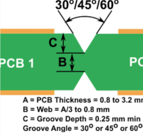
Firstly, the depth of the V-cut is a critical parameter that must be carefully controlled.
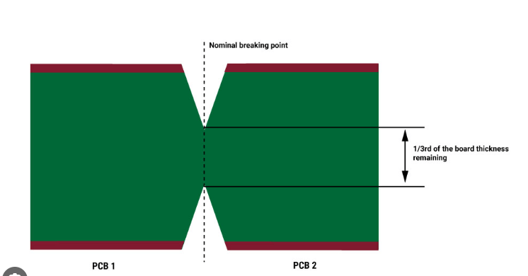
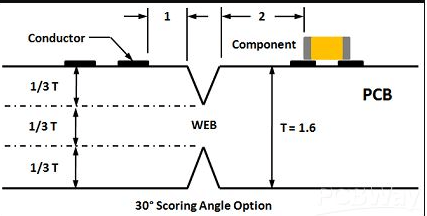
The depth determines how easily the boards can be separated without causing damage to the components or the board itself. Typically, the V-cut depth is set to penetrate approximately one-third to one-half of the board’s thickness. This ensures that the boards remain securely attached during assembly but can be easily snapped apart when needed. Deviating from the recommended depth can lead to issues such as incomplete separation or excessive stress on the board, potentially compromising its integrity.
In addition to depth, the angle of the V-cut is another vital specification.
The standard angle for V-cuts is usually 30 to 45 degrees, which provides a balance between ease of separation and structural stability. A steeper angle may result in a weaker connection between the boards, increasing the risk of accidental separation during handling. Conversely, a shallower angle might make it more challenging to break the boards apart cleanly, leading to rough edges or damage. Therefore, maintaining the correct angle is essential for achieving a smooth and efficient separation process.
Spacing between V-cuts is also a crucial consideration in PCB design.
The spacing must be sufficient to accommodate the components and traces on the board while allowing for easy separation. Typically, a minimum spacing of 0.5 mm to 1 mm is recommended to ensure that the V-cuts do not interfere with the board’s functionality. However, the exact spacing may vary depending on the specific requirements of the design and the manufacturing process. It is essential to collaborate with the PCB manufacturer to determine the optimal spacing for each project.
Moreover, it is important to consider the material properties of the PCB when specifying V-cuts.
Different materials, such as FR4, polyimide, or metal-core PCBs, may respond differently to the V-cut process. For instance, FR4, a commonly used material, is relatively easy to score and snap, while metal-core PCBs may require more precise control of the V-cut parameters to avoid damaging the metal layer. Understanding the material characteristics and adjusting the V-cut specifications accordingly can help achieve the desired results without compromising the board’s performance.
In conclusion, understanding PCB V-cut specifications is essential for ensuring the quality and efficiency of the manufacturing process. By carefully controlling parameters such as depth, angle, and spacing, engineers and manufacturers can achieve precise and reliable separation of individual boards. Additionally, considering the material properties of the PCB and collaborating with the manufacturer can further enhance the effectiveness of the V-cut process. Adhering to these specifications not only improves the overall quality of the PCBs but also contributes to the success of the final electronic products.
Key Factors Influencing PCB V-Cut Quality
Printed Circuit Boards (PCBs) are integral components in modern electronic devices, and their manufacturing process involves various intricate steps to ensure optimal performance and reliability. One such critical step is the V-cut, a technique used to create a groove in the PCB, allowing for easy separation of individual boards from a larger panel. The quality of the V-cut significantly impacts the overall functionality and durability of the PCB, making it essential to understand the key factors influencing this process.
Firstly, the precision of the V-cut machinery plays a pivotal role in determining the quality of the cut.
Advanced V-cut machines equipped with high-precision blades and accurate control systems ensure that the grooves are consistent and meet the specified dimensions. Any deviation in the machinery’s calibration can lead to uneven cuts, which may compromise the structural integrity of the PCB. Therefore, regular maintenance and calibration of the V-cut equipment are crucial to achieving high-quality results.
Another important factor is the material composition of the PCB.
Different materials exhibit varying degrees of hardness and brittleness, which can affect the ease and quality of the V-cut. For instance, PCBs made from FR4, a common fiberglass-reinforced epoxy laminate, require specific blade types and cutting speeds to achieve a clean cut without causing delamination or cracking. Understanding the material properties and selecting the appropriate cutting parameters are essential to maintaining the integrity of the PCB during the V-cut process.
The thickness of the PCB also significantly influences the V-cut quality.
Thicker PCBs require deeper grooves to ensure they can be easily separated without excessive force, which could damage the board or its components. Conversely, thinner PCBs are more susceptible to bending and warping during the cutting process, necessitating precise control over the cutting depth and speed. Manufacturers must carefully consider the PCB thickness and adjust their V-cut parameters accordingly to achieve optimal results.
Moreover, the design and layout of the PCB can impact the V-cut quality.
The placement of components and traces near the V-cut line must be carefully planned to avoid potential damage during the separation process. Components placed too close to the V-cut line may be subjected to mechanical stress, leading to solder joint failures or component dislodgement. Therefore, designers must collaborate closely with manufacturers to ensure that the PCB layout accommodates the V-cut process without compromising the board’s functionality.
Additionally, the cleanliness of the PCB surface before and after the V-cut process is vital.
Any debris or contaminants on the PCB surface can interfere with the cutting process, leading to rough or uneven cuts. Post-cut cleaning is equally important to remove any residual particles that could affect the board’s performance or cause short circuits. Implementing stringent cleaning protocols and using appropriate cleaning agents can help maintain the quality of the V-cut and the overall PCB.
Lastly, the experience and skill of the operators handling the V-cut machinery cannot be overlooked.
Skilled operators with a thorough understanding of the V-cut process and its nuances can make real-time adjustments to the machinery settings, ensuring consistent and high-quality cuts. Continuous training and knowledge updates for operators are essential to keep pace with advancements in V-cut technology and techniques.
In conclusion, achieving high-quality V-cuts in PCB manufacturing is a multifaceted process influenced by machinery precision, material properties, PCB thickness, design considerations, surface cleanliness, and operator expertise. By meticulously addressing these factors, manufacturers can ensure that the V-cut process enhances the overall quality and reliability of the PCBs, ultimately contributing to the success of electronic devices in various applications.
Common Mistakes to Avoid in PCB V-Cut Design
In the realm of printed circuit board (PCB) manufacturing, the V-cut process is a critical step that facilitates the separation of individual boards from a larger panel. However, despite its importance, several common mistakes can compromise the integrity and functionality of the final product. Understanding these pitfalls is essential for engineers and designers aiming to optimize their PCB V-cut designs.
One prevalent mistake is the improper alignment of the V-cut lines.
Misalignment can lead to uneven edges, which not only affects the aesthetic quality of the boards but also poses a risk to their structural integrity. To avoid this, it is crucial to ensure that the V-cut lines are precisely aligned with the intended separation points. Utilizing advanced design software and double-checking measurements can significantly mitigate this issue.
Another frequent error involves the depth of the V-cut.
If the cut is too shallow, it may not sufficiently weaken the material, making it difficult to separate the boards without causing damage. Conversely, a cut that is too deep can compromise the board’s strength, leading to potential breakage during handling or assembly. Therefore, it is essential to adhere to the recommended depth specifications, typically around one-third to one-half of the board’s thickness, to achieve an optimal balance between ease of separation and structural integrity.
Moreover, the spacing between V-cuts is a critical factor that is often overlooked.
Insufficient spacing can result in excessive stress on the boards during separation, increasing the likelihood of cracks or fractures. On the other hand, excessive spacing can lead to wasted material and increased production costs. To strike the right balance, designers should follow industry guidelines and consider the specific requirements of their project, ensuring that the spacing is neither too tight nor too loose.
In addition to spacing, the angle of the V-cut is another aspect that demands careful consideration.
A common mistake is using an inappropriate angle, which can affect the ease of separation and the quality of the edge finish. Typically, a 30 to 45-degree angle is recommended for most applications, as it provides a good compromise between ease of separation and edge quality. However, it is important to tailor the angle to the specific needs of the project, taking into account factors such as board thickness and material type.
Furthermore, neglecting to account for the impact of the V-cut on the board’s electrical performance is a mistake that can have serious consequences.
The V-cut process can introduce stress points and potential weak spots that may affect the board’s reliability and longevity. To mitigate this risk, designers should conduct thorough stress analysis and consider reinforcing critical areas with additional support structures or alternative design strategies.
Lastly, inadequate communication between the design and manufacturing teams can lead to misunderstandings and errors in the V-cut process.
Clear and detailed documentation, including precise specifications and tolerances, is essential to ensure that the manufacturing team accurately executes the design intent. Regular collaboration and feedback loops between the teams can further enhance the quality and consistency of the final product.
In conclusion, avoiding common mistakes in PCB V-cut design requires meticulous attention to detail and a thorough understanding of the various factors involved. By ensuring proper alignment, depth, spacing, angle, and considering the impact on electrical performance, designers can significantly improve the quality and reliability of their PCBs. Additionally, fostering effective communication between design and manufacturing teams is crucial to achieving optimal results. Through these practices, the potential pitfalls of the V-cut process can be effectively mitigated, leading to superior PCB performance and durability.
Comparing PCB V-Cut and Other Depaneling Methods
When it comes to the manufacturing of printed circuit boards (PCBs), the depaneling process is a critical step that ensures individual boards are separated from a larger panel without causing damage. Among the various depaneling methods available, PCB V-Cut stands out for its unique advantages and specific applications. However, to fully appreciate its benefits, it is essential to compare it with other prevalent depaneling techniques such as routing, laser cutting, and punching.
PCB V-Cut, also known as V-scoring, involves making a V-shaped groove along the lines where the PCB will be separated.
This groove is typically made on both sides of the board, allowing for easy snapping apart of the individual units. One of the primary advantages of V-Cut is its cost-effectiveness. The process is relatively simple and does not require expensive machinery, making it an attractive option for manufacturers looking to minimize production costs. Additionally, V-Cut is highly efficient for high-volume production runs, as it allows for quick and easy separation of multiple boards.
In contrast, routing involves using a CNC machine to cut out the individual PCBs from the panel.
This method is highly precise and can handle complex board shapes that V-Cut cannot accommodate. However, routing is generally more time-consuming and expensive due to the need for specialized equipment and the longer processing time. The precision of routing makes it ideal for applications where the board design includes intricate patterns or where maintaining the integrity of the board edges is crucial.
Laser cutting is another advanced depaneling method that offers unparalleled precision and flexibility.
Using a high-powered laser, this technique can cut through various materials with minimal mechanical stress, reducing the risk of damaging sensitive components. Laser cutting is particularly beneficial for boards with delicate or densely packed components, as it minimizes the risk of mechanical stress and potential damage. However, the high cost of laser cutting equipment and the slower processing speed compared to V-Cut can be significant drawbacks for some manufacturers.
Punching, on the other hand, is a method that uses a die and punch to separate the PCBs from the panel.
This technique is highly efficient for high-volume production and can produce clean, precise cuts. However, the initial cost of creating custom dies can be prohibitive, especially for small production runs or prototypes. Additionally, punching is less flexible than other methods, as it requires a new die for each different board design.
When comparing PCB V-Cut to these other depaneling methods, it becomes clear that each technique has its own set of advantages and limitations.
V-Cut is particularly well-suited for straightforward, high-volume production runs where cost and efficiency are paramount. Its simplicity and low cost make it an attractive option for many manufacturers. However, for more complex board designs or applications requiring high precision and minimal mechanical stress, routing, laser cutting, or punching may be more appropriate.
In conclusion, the choice of depaneling method depends largely on the specific requirements of the PCB design and the production volume. While PCB V-Cut offers a cost-effective and efficient solution for many applications, other methods like routing, laser cutting, and punching provide alternatives that may be better suited to more complex or delicate designs. By carefully considering the advantages and limitations of each method, manufacturers can select the most appropriate depaneling technique to meet their specific needs.