Pcb v-cut
Understanding The Basics Of PCB V-Cut
Printed Circuit Boards (PCBs) are integral components in modern electronic devices, serving as the backbone that connects various electronic components. Among the numerous techniques employed in PCB manufacturing, the V-cut process stands out for its efficiency and precision. Understanding the basics of PCB V-cut is essential for anyone involved in electronics design and manufacturing.
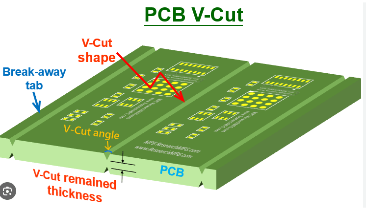
The V-cut, also known as V-groove, is a method used to separate individual PCBs from a larger panel.
This technique involves making a V-shaped groove along the lines where the boards will be separated. The grooves are typically cut at a 30 to 45-degree angle, creating a weakened line that allows for easy breaking or snapping of the boards. This method is particularly advantageous in high-volume production environments where efficiency and precision are paramount.
One of the primary benefits of the V-cut process is its ability to maintain the structural integrity of the PCBs.
Unlike other separation methods, such as routing or punching, V-cutting minimizes stress on the boards. This is crucial in preventing damage to delicate components and maintaining the overall quality of the final product. Additionally, the V-cut process is highly efficient, allowing for the simultaneous separation of multiple boards, which significantly reduces production time and costs.
Transitioning to the technical aspects, the V-cut process requires specialized equipment.
CNC (Computer Numerical Control) machines are commonly used to ensure precision and consistency. These machines are programmed to cut the grooves at specific depths and angles, tailored to the design requirements of the PCBs. The accuracy of CNC machines ensures that the grooves are uniform, which is essential for the reliable separation of the boards.
Moreover, the V-cut process is versatile and can be applied to various types of PCBs, including single-sided, double-sided, and multi-layer boards.
This versatility makes it a preferred choice for a wide range of applications, from consumer electronics to industrial equipment. However, it is important to note that the V-cut process is not suitable for all PCB designs. For instance, boards with components placed too close to the edge may not be ideal candidates for V-cutting, as the process could potentially damage the components.
In addition to its technical advantages, the V-cut process also offers economic benefits.
By reducing the need for additional handling and processing steps, manufacturers can achieve significant cost savings. The ability to produce multiple boards from a single panel also optimizes material usage, further contributing to cost efficiency. These economic advantages make the V-cut process an attractive option for manufacturers looking to streamline their production processes.
Furthermore, the V-cut process aligns with the growing emphasis on sustainability in manufacturing.
By optimizing material usage and reducing waste, this method supports environmentally friendly practices. As the electronics industry continues to evolve, the adoption of sustainable manufacturing techniques will become increasingly important.
In conclusion, understanding the basics of PCB V-cut is essential for anyone involved in electronics design and manufacturing. This process offers numerous benefits, including maintaining structural integrity, efficiency, versatility, and cost savings. With the use of specialized equipment and careful consideration of design requirements, the V-cut process can significantly enhance the quality and efficiency of PCB production. As the industry continues to advance, the V-cut method will undoubtedly remain a valuable tool in the manufacturing of high-quality electronic devices.
Advantages And Disadvantages Of PCB V-Cut
Printed Circuit Boards (PCBs) are fundamental components in modern electronic devices, and their design and manufacturing processes are critical to the performance and reliability of the final product. One of the techniques used in PCB manufacturing is the V-cut, also known as V-groove, which involves cutting a V-shaped groove into the board to facilitate its separation into individual units. This method offers several advantages and disadvantages that are important to consider.
One of the primary advantages of PCB V-cut is its efficiency in the manufacturing process.
By using V-cuts, multiple PCBs can be produced on a single panel and then easily separated, which significantly reduces handling time and increases production throughput. This method is particularly beneficial for high-volume production runs where time and cost savings are paramount. Additionally, V-cuts allow for precise and clean separations, which can be crucial for maintaining the integrity of the board edges and ensuring that the final product meets stringent quality standards.
Another significant benefit of the V-cut technique is its ability to maximize the use of available space on a PCB panel.
By arranging the boards in a way that minimizes waste, manufacturers can optimize material usage, leading to cost savings and a more environmentally friendly production process. This efficient use of space is especially important in industries where miniaturization and compact design are critical, such as in consumer electronics and medical devices.
However, despite these advantages, there are also notable disadvantages associated with PCB V-cuts.
One of the main drawbacks is the potential for mechanical stress on the boards during the separation process. The act of breaking the boards apart along the V-groove can introduce stress fractures or micro-cracks, which may compromise the structural integrity and reliability of the PCB. This issue is particularly concerning for boards that will be subjected to mechanical or thermal stress during their operational life.
Moreover, the V-cut technique can limit the design flexibility of the PCB.
The need to create straight, continuous grooves means that certain complex or irregular board shapes may not be feasible. This limitation can be a significant drawback for applications that require custom or intricate PCB designs. Additionally, the V-cut process may not be suitable for very thin or delicate boards, as the separation process could damage them.
Another consideration is the potential impact on the electrical performance of the PCB.
The V-groove can introduce variations in the board’s thickness, which may affect the impedance and signal integrity of high-frequency circuits. This issue is particularly relevant for applications in telecommunications and high-speed computing, where maintaining precise electrical characteristics is crucial.
In conclusion, while PCB V-cut offers several advantages, including increased manufacturing efficiency, optimized material usage, and clean separations, it also presents challenges such as potential mechanical stress, limited design flexibility, and possible impacts on electrical performance. Manufacturers must carefully weigh these factors when deciding whether to use the V-cut technique for their specific applications. By understanding both the benefits and drawbacks, they can make informed decisions that balance production efficiency with the quality and reliability of the final product.
How To Design PCBs For Optimal V-Cut Performance
Designing printed circuit boards (PCBs) for optimal V-cut performance requires a meticulous approach to ensure both functionality and manufacturability. V-cuts, or V-grooves, are essential in PCB manufacturing as they facilitate the separation of individual boards from a larger panel. To achieve optimal V-cut performance, several critical factors must be considered during the design phase.
Firstly, understanding the purpose and application of V-cuts is paramount.
V-cuts are typically used in high-volume production where multiple PCBs are fabricated on a single panel and then separated. This method is advantageous as it reduces handling time and minimizes the risk of damaging individual boards. Consequently, the design must accommodate the V-cut process without compromising the integrity of the PCBs.
One of the primary considerations in designing for V-cuts is the placement of components and traces.
Components should be positioned at a safe distance from the V-cut lines to prevent damage during the separation process. A general rule of thumb is to maintain a minimum clearance of 0.5mm from the V-cut line to any component or trace. This buffer zone ensures that the mechanical stress exerted during the separation does not affect the components or the electrical performance of the board.
In addition to component placement, the layout of the PCB traces must be carefully planned.
Traces that run parallel to the V-cut lines are particularly vulnerable to stress and potential damage. Therefore, it is advisable to route traces perpendicular to the V-cut lines whenever possible. If parallel routing is unavoidable, reinforcing the traces with additional copper or using wider traces can mitigate the risk of damage.
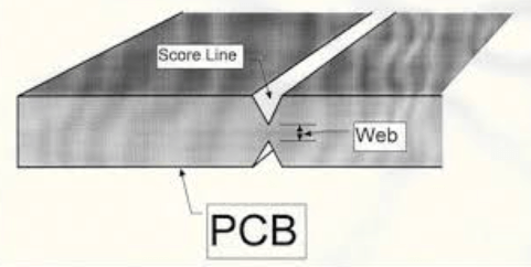
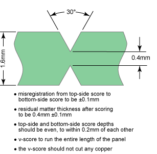
Another crucial aspect is the thickness of the PCB.
The depth of the V-cut is typically half the thickness of the board, creating a V-shaped groove that facilitates easy separation. Therefore, the board thickness must be consistent and within the specified tolerance to ensure uniform V-cuts. Variations in board thickness can lead to inconsistent V-cuts, making the separation process difficult and potentially damaging the boards.
Furthermore, the choice of materials plays a significant role in V-cut performance.
High-quality materials with consistent thickness and minimal warpage are essential for achieving precise V-cuts. Materials with poor dimensional stability can lead to misalignment and uneven V-cuts, compromising the separation process and the overall quality of the PCBs.
The design of the panel itself also warrants careful consideration.
The panel should be designed to maximize the number of PCBs while maintaining sufficient space for the V-cuts. Additionally, incorporating fiducial marks and alignment holes can aid in the accurate placement of V-cuts, ensuring that each board is separated cleanly and without damage.
Moreover, collaboration with the PCB manufacturer during the design phase can provide valuable insights into optimizing V-cut performance.
Manufacturers can offer guidance on the best practices for V-cut design, including recommendations on panelization, material selection, and trace routing. Engaging with the manufacturer early in the design process can help identify potential issues and implement solutions before production begins.
In conclusion, designing PCBs for optimal V-cut performance involves a comprehensive approach that considers component placement, trace routing, board thickness, material selection, and panel design. By adhering to these guidelines and collaborating with the manufacturer, designers can ensure that their PCBs are not only functional but also manufacturable, resulting in high-quality boards that meet the demands of modern electronic applications.
Common Mistakes To Avoid In PCB V-Cut Manufacturing
In the realm of printed circuit board (PCB) manufacturing, the V-cut process is a critical step that facilitates the separation of individual boards from a larger panel. However, despite its importance, several common mistakes can occur during PCB V-cut manufacturing, which can compromise the integrity and functionality of the final product. Understanding these pitfalls and how to avoid them is essential for ensuring high-quality outcomes.
One prevalent mistake in PCB V-cut manufacturing is improper alignment.
Accurate alignment is crucial because even a slight deviation can lead to misaligned cuts, which can affect the dimensions and fit of the individual boards. To avoid this, it is essential to use precise alignment tools and regularly calibrate the equipment. Additionally, implementing a robust quality control process that includes regular inspections can help identify and correct alignment issues before they become problematic.
Another common error is incorrect depth of the V-cut.
The depth of the cut must be carefully controlled to ensure that the boards can be easily separated without damaging the components or the board itself. If the cut is too shallow, it may be difficult to break the boards apart, leading to potential damage during separation. Conversely, if the cut is too deep, it can weaken the structural integrity of the board, making it more susceptible to breakage during handling and assembly. To mitigate this risk, manufacturers should use precise cutting tools and regularly monitor the depth of the cuts to ensure consistency.
Moreover, the choice of cutting tools and their maintenance play a significant role in the quality of the V-cut.
Dull or worn-out blades can result in rough edges and burrs, which can interfere with the assembly process and lead to poor electrical connections. Therefore, it is imperative to use high-quality cutting tools and maintain them properly. Regularly sharpening or replacing blades can help achieve clean, precise cuts, thereby enhancing the overall quality of the PCB.
In addition to the technical aspects, material selection is another critical factor that can influence the success of the V-cut process.
Different PCB materials have varying properties, such as hardness and brittleness, which can affect how they respond to cutting. Using the wrong material can lead to issues such as cracking or delamination during the V-cut process. To avoid this, manufacturers should carefully select materials that are compatible with the V-cut process and consider conducting material tests to ensure suitability.
Furthermore, inadequate consideration of the board layout can also lead to problems during the V-cut process.
Placing components too close to the V-cut line can result in damage to the components during separation. To prevent this, it is essential to design the PCB layout with sufficient clearance between the V-cut line and the components. This not only protects the components but also ensures that the boards can be separated cleanly and efficiently.
Lastly, overlooking the importance of proper documentation and communication can lead to errors in the V-cut process.
Clear and detailed documentation of the V-cut specifications, including alignment, depth, and layout considerations, is crucial for ensuring that all team members are on the same page. Effective communication between the design and manufacturing teams can help identify potential issues early in the process and facilitate timely resolution.
In conclusion, avoiding common mistakes in PCB V-cut manufacturing requires a combination of precise alignment, controlled cutting depth, proper tool maintenance, careful material selection, thoughtful board layout, and effective documentation and communication. By paying attention to these factors, manufacturers can enhance the quality and reliability of their PCBs, ultimately leading to better performance and customer satisfaction.