Pcb rf filter design
Understanding The Basics Of PCB RF Filter Design
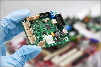
Printed Circuit Board (PCB) Radio Frequency (RF) filter design is a critical aspect of modern electronics, particularly in applications involving communication systems, signal processing, and wireless technologies. Understanding the basics of PCB RF filter design requires a grasp of both theoretical principles and practical considerations. This article aims to elucidate these foundational elements, providing a comprehensive overview for those interested in the field.
To begin with, RF filters are essential components that allow certain frequencies to pass while attenuating others.
They are used to eliminate unwanted signals and noise, thereby ensuring the integrity and clarity of the desired signal. The design of these filters on a PCB involves a meticulous process that balances electrical performance with physical constraints.
One of the primary considerations in PCB RF filter design is the selection of the filter type.
Common types include low-pass, high-pass, band-pass, and band-stop filters. Each type serves a specific purpose, depending on the frequency range that needs to be isolated or passed. For instance, a low-pass filter allows frequencies below a certain cutoff point to pass through while attenuating higher frequencies. Conversely, a high-pass filter does the opposite. Band-pass and band-stop filters are more specialized, allowing or rejecting a specific range of frequencies, respectively.
Transitioning from the theoretical to the practical, the next step involves the choice of components and materials.
The performance of an RF filter is heavily influenced by the quality and characteristics of the components used, such as inductors, capacitors, and resistors. These components must be selected based on their frequency response, tolerance, and stability. Additionally, the substrate material of the PCB itself plays a crucial role. Materials with low dielectric loss and stable dielectric constants are preferred to minimize signal degradation and ensure consistent performance across the desired frequency range.
Another critical aspect is the layout of the PCB.
The physical arrangement of components and the routing of traces can significantly impact the filter’s performance. For instance, minimizing the length of signal paths and avoiding sharp bends can reduce inductive and capacitive parasitics, which can otherwise distort the signal. Moreover, proper grounding and shielding techniques are essential to mitigate electromagnetic interference (EMI) and crosstalk between adjacent traces.
Simulation and testing are indispensable steps in the design process.
Before finalizing the PCB layout, designers typically use simulation software to model the filter’s behavior and predict its performance. These simulations help identify potential issues and allow for adjustments to be made before the physical prototype is created. Once the prototype is built, rigorous testing is conducted to verify that the filter meets the desired specifications. This testing often involves measuring parameters such as insertion loss, return loss, and bandwidth to ensure the filter performs as intended.
In conclusion, PCB RF filter design is a multifaceted discipline that requires a deep understanding of both theoretical principles and practical considerations. From selecting the appropriate filter type and components to optimizing the PCB layout and conducting thorough testing, each step is crucial to achieving a high-performance RF filter. By mastering these basics, designers can create filters that effectively manage signal integrity and contribute to the overall success of electronic systems.

Key Considerations For Effective PCB RF Filter Layout
Designing an effective PCB RF filter layout requires meticulous attention to detail and a comprehensive understanding of various key considerations. The performance of RF filters is highly dependent on the layout of the printed circuit board (PCB), which can significantly influence signal integrity, noise levels, and overall system efficiency. Therefore, it is essential to address several critical factors to ensure optimal functionality.
Firstly, the choice of materials plays a pivotal role in the performance of RF filters.
High-frequency signals are particularly sensitive to the dielectric properties of the PCB substrate. Materials with low dielectric constant (Dk) and low loss tangent (Df) are preferred, as they minimize signal attenuation and phase distortion. Commonly used materials include Rogers, Teflon, and other specialized RF substrates, which offer superior performance compared to standard FR4.
In addition to material selection, the layout of the traces is crucial.
The width, length, and spacing of the traces must be carefully designed to maintain the characteristic impedance and minimize signal reflections. Microstrip and stripline configurations are commonly used in RF designs due to their predictable impedance characteristics. Ensuring that the traces are as short and direct as possible helps to reduce inductive and capacitive parasitics, which can degrade filter performance.
Moreover, grounding is a fundamental aspect of RF filter design. A solid and continuous ground plane is essential to provide a low-impedance return path for RF signals.
This helps to reduce electromagnetic interference (EMI) and crosstalk between adjacent traces. Vias should be strategically placed to connect the ground plane to the top and bottom layers, ensuring a robust grounding system. Additionally, the use of ground stitching vias around the filter components can further enhance isolation and reduce noise.
Component placement is another critical consideration.
RF components, such as inductors and capacitors, should be placed as close to each other as possible to minimize parasitic inductance and capacitance. This proximity helps to maintain the desired filter characteristics and improves overall performance. Furthermore, it is advisable to place sensitive components away from high-power or noisy sections of the PCB to prevent unwanted coupling and interference.
Thermal management is also an important factor in RF filter design.
High-frequency components can generate significant heat, which can affect their performance and reliability. Proper thermal vias and heat sinks should be incorporated into the design to dissipate heat effectively. Additionally, maintaining adequate spacing between components can help to prevent thermal buildup and ensure consistent performance.
Transitioning to the topic of simulation and testing, it is imperative to use advanced simulation tools during the design phase.
Electromagnetic (EM) simulation software can model the behavior of RF signals on the PCB, allowing designers to identify and mitigate potential issues before fabrication. Post-fabrication testing is equally important to verify the performance of the RF filter. Network analyzers and spectrum analyzers are commonly used to measure parameters such as insertion loss, return loss, and bandwidth, ensuring that the filter meets the desired specifications.
In conclusion, designing an effective PCB RF filter layout involves a careful balance of material selection, trace layout, grounding, component placement, thermal management, and thorough testing. By addressing these key considerations, designers can achieve optimal performance and reliability in their RF filter designs, ultimately contributing to the success of the overall system.
Common Mistakes To Avoid In PCB RF Filter Design
Designing RF filters on printed circuit boards (PCBs) is a critical task that requires meticulous attention to detail. However, even experienced engineers can fall prey to common mistakes that can compromise the performance of the RF filter. One prevalent error is the improper selection of materials. The dielectric constant and loss tangent of the PCB substrate significantly influence the filter’s performance. Using a substrate with a high dielectric constant can lead to increased signal loss and reduced filter efficiency. Therefore, it is essential to choose materials that offer low dielectric loss and are suitable for high-frequency applications.
Another frequent mistake is inadequate grounding.
A poor grounding scheme can introduce noise and unwanted signals, thereby degrading the filter’s performance. Ensuring a solid ground plane and minimizing ground loops are crucial steps in mitigating these issues. Additionally, the placement of vias and the use of multiple ground layers can further enhance grounding effectiveness.
Transitioning to layout considerations, the physical placement of components is another area where errors often occur.
Placing components too close to each other can lead to unwanted coupling and interference. Conversely, placing them too far apart can introduce parasitic inductance and capacitance, which can alter the filter’s characteristics. Therefore, maintaining an optimal distance between components is vital for achieving the desired filter performance.
Moreover, the trace width and spacing are critical parameters that should not be overlooked.
Narrow traces can increase resistance and cause signal attenuation, while wide traces can introduce parasitic capacitance. Similarly, inadequate spacing between traces can lead to crosstalk and signal degradation. Utilizing impedance-controlled traces and adhering to design guidelines can help mitigate these issues.
Transitioning to the topic of simulation, relying solely on theoretical calculations without validating the design through simulation is a common pitfall.
Simulation tools can provide valuable insights into the filter’s performance and help identify potential issues before fabrication. Therefore, incorporating simulation into the design process is highly recommended.
Another mistake to avoid is neglecting the impact of temperature variations.
Temperature changes can affect the dielectric properties of the substrate and the performance of passive components, leading to shifts in the filter’s frequency response. Therefore, it is essential to consider temperature stability during the design phase and select components that offer minimal variation with temperature.
Furthermore, the use of inappropriate or low-quality components can severely impact the filter’s performance.
Components such as inductors and capacitors should be chosen based on their frequency characteristics and quality factors. Using components with low Q-factors can introduce significant losses and degrade the filter’s efficiency. Therefore, selecting high-quality components that meet the design specifications is crucial.
Lastly, inadequate testing and validation can lead to unforeseen issues in the final product.
Comprehensive testing, including S-parameter measurements and time-domain analysis, can help verify the filter’s performance and ensure it meets the design requirements. Skipping these steps can result in a filter that does not perform as intended, leading to costly redesigns and delays.
In conclusion, avoiding these common mistakes in PCB RF filter design requires a thorough understanding of material properties, grounding techniques, component placement, trace design, simulation, temperature effects, component selection, and testing. By paying careful attention to these aspects, engineers can design RF filters that perform reliably and efficiently in their intended applications.
Advanced Techniques For Optimizing PCB RF Filter Performance
In the realm of high-frequency electronics, the design of printed circuit board (PCB) radio frequency (RF) filters is a critical task that demands precision and expertise. These filters are essential for ensuring signal integrity, minimizing interference, and enhancing overall system performance. To achieve optimal results, advanced techniques must be employed, each contributing to the refinement of the filter’s performance.
One of the foremost considerations in PCB RF filter design is the selection of appropriate materials.
The dielectric constant and loss tangent of the substrate material significantly influence the filter’s performance. Low-loss materials, such as PTFE or ceramic-filled laminates, are often preferred due to their ability to minimize signal attenuation and maintain high Q-factors. Additionally, the thickness of the substrate must be carefully chosen to balance mechanical stability and electrical performance.
Transitioning from material selection, the next critical aspect is the layout of the PCB.
The physical arrangement of components and traces can have a profound impact on the filter’s characteristics. To mitigate parasitic effects, it is essential to maintain consistent trace widths and spacing, particularly in high-frequency applications. Ground planes should be strategically placed to provide a low-impedance return path and reduce electromagnetic interference (EMI). Furthermore, the use of via stitching can enhance grounding and improve overall signal integrity.
Another advanced technique involves the meticulous design of the filter’s topology.
Various filter configurations, such as Butterworth, Chebyshev, and elliptic filters, offer distinct advantages depending on the application requirements. For instance, Butterworth filters provide a maximally flat passband, making them suitable for applications where signal fidelity is paramount. In contrast, Chebyshev filters offer steeper roll-off characteristics, which are advantageous in scenarios where sharp cutoff frequencies are needed. The choice of topology must be aligned with the specific performance criteria of the RF system.
Moreover, the implementation of electromagnetic simulation tools is indispensable in modern PCB RF filter design.
These tools enable designers to model and analyze the electromagnetic behavior of the filter, allowing for the identification and mitigation of potential issues before physical prototyping. By leveraging simulation software, designers can optimize the filter’s performance parameters, such as insertion loss, return loss, and bandwidth, with a high degree of accuracy. This iterative process of simulation and refinement is crucial for achieving the desired filter characteristics.
In addition to simulation, the use of advanced manufacturing techniques can further enhance the performance of PCB RF filters.
Precision etching and laser drilling enable the creation of intricate geometries and fine features that are essential for high-frequency applications. These techniques also facilitate the integration of surface-mount components, which can reduce parasitic inductance and capacitance, thereby improving the filter’s overall performance.
Finally, thorough testing and validation are imperative to ensure that the designed filter meets the specified performance criteria. Network analyzers and spectrum analyzers are commonly used to measure key parameters such as insertion loss, return loss, and group delay. By conducting comprehensive testing, designers can verify the filter’s performance and make any necessary adjustments to achieve optimal results.
In conclusion, optimizing PCB RF filter performance requires a multifaceted approach that encompasses material selection, layout design, topology choice, electromagnetic simulation, advanced manufacturing techniques, and rigorous testing. By employing these advanced techniques, designers can create high-performance RF filters that meet the stringent demands of modern high-frequency applications.