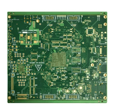
Pcb prototype device
Understanding The Basics Of PCB Prototype Devices
Printed Circuit Board (PCB) prototype devices are essential tools in the development and testing of electronic circuits. These devices serve as preliminary versions of the final PCB, allowing engineers and designers to evaluate the functionality, performance, and reliability of their designs before mass production. Understanding the basics of PCB prototype devices is crucial for anyone involved in electronics design and manufacturing.
To begin with, a PCB prototype is a model of the final circuit board, created to test and validate the design.
This prototype is typically produced using the same materials and processes as the final product, ensuring that the test results are accurate and reliable. The primary purpose of a PCB prototype is to identify and rectify any design flaws, thereby reducing the risk of costly errors in the final production run. By thoroughly testing the prototype, designers can make necessary adjustments to improve the overall performance and reliability of the circuit.
One of the key aspects of PCB prototype devices is the design process.
This process involves several stages, starting with the creation of a schematic diagram. The schematic diagram is a detailed representation of the electronic circuit, showing all the components and their connections. Once the schematic is complete, it is converted into a layout design, which specifies the physical arrangement of the components on the PCB. The layout design is then used to create the actual prototype, either through traditional manufacturing methods or advanced techniques such as 3D printing.
Transitioning to the next stage, the manufacturing of PCB prototypes can be done using various methods, each with its own advantages and limitations.
Traditional methods, such as etching and milling, are widely used due to their accuracy and reliability. However, these methods can be time-consuming and expensive, especially for complex designs. On the other hand, modern techniques like 3D printing offer a faster and more cost-effective alternative, allowing for rapid prototyping and iterative testing. Regardless of the method used, the goal is to produce a high-quality prototype that closely resembles the final product.
Once the PCB prototype is manufactured, it undergoes a series of tests to evaluate its performance.
These tests include functional testing, where the prototype is powered on and its operation is verified, and environmental testing, where the prototype is subjected to various conditions such as temperature and humidity to assess its durability. Additionally, electrical testing is performed to check for issues like short circuits and open circuits. By conducting these tests, designers can identify any potential problems and make necessary adjustments to the design.
Furthermore, the feedback obtained from testing the PCB prototype is invaluable for refining the design.
This iterative process of testing and modification helps to ensure that the final product meets all the required specifications and performs reliably in real-world conditions. It also allows designers to experiment with different components and configurations, ultimately leading to a more optimized and efficient design.
In conclusion, PCB prototype devices play a critical role in the development of electronic circuits. They provide a means for designers to test and validate their designs, identify and rectify any issues, and refine the final product. By understanding the basics of PCB prototype devices, engineers and designers can leverage these tools to create high-quality, reliable electronic products. The iterative process of prototyping, testing, and modification is essential for achieving optimal performance and ensuring the success of the final product in the market.
Top Benefits Of Using PCB Prototype Devices In Product Development
In the realm of product development, the utilization of PCB prototype devices has become increasingly indispensable. These devices offer a myriad of benefits that significantly enhance the efficiency and effectiveness of the development process. One of the foremost advantages is the ability to identify and rectify design flaws at an early stage. By creating a prototype, engineers can test the functionality of the circuit and ensure that it meets the desired specifications. This early detection of issues not only saves time but also reduces the cost associated with making changes to the design later in the development cycle.
Moreover, PCB prototype devices facilitate a more streamlined and iterative design process.
With the ability to quickly produce and test multiple iterations of a design, engineers can experiment with different configurations and components to optimize performance. This iterative approach allows for continuous improvement and refinement, leading to a more robust and reliable final product. Additionally, the use of prototypes enables better communication and collaboration among team members, as tangible models can be used to convey ideas and concepts more effectively than abstract diagrams or descriptions.
Another significant benefit of using PCB prototype devices is the acceleration of the development timeline.
Traditional methods of circuit design and testing can be time-consuming and labor-intensive. In contrast, modern prototyping techniques, such as 3D printing and automated assembly, allow for rapid production of prototypes. This speed not only shortens the overall development cycle but also enables faster response to market demands and technological advancements. Consequently, companies can bring their products to market more quickly, gaining a competitive edge in the industry.
Furthermore, PCB prototype devices play a crucial role in ensuring the manufacturability of a design.
By creating a prototype, engineers can assess the feasibility of mass production and identify any potential challenges that may arise during the manufacturing process. This preemptive evaluation helps to mitigate risks and avoid costly delays or rework once production begins. Additionally, prototypes can be used to validate the performance and reliability of a design under real-world conditions, providing valuable insights that inform the final production process.
In addition to these practical benefits, PCB prototype devices also contribute to cost savings in product development.
By identifying and addressing design flaws early, companies can avoid the expenses associated with late-stage modifications or recalls. Moreover, the ability to test and refine designs through multiple iterations reduces the likelihood of costly errors and ensures that the final product meets the highest standards of quality and performance. This cost-effectiveness is particularly important in industries where margins are tight and competition is fierce.
Lastly, the use of PCB prototype devices fosters innovation and creativity in product development.
By providing a tangible platform for experimentation and exploration, prototypes encourage engineers to push the boundaries of what is possible and develop novel solutions to complex problems. This spirit of innovation not only leads to better products but also drives progress and growth within the industry as a whole.
In conclusion, the benefits of using PCB prototype devices in product development are manifold. From early detection of design flaws and iterative improvement to accelerated timelines and cost savings, these devices play a pivotal role in enhancing the efficiency and effectiveness of the development process. Moreover, they foster innovation and ensure the manufacturability and reliability of the final product. As such, PCB prototype devices are an invaluable tool for any company seeking to excel in the competitive landscape of modern product development.
Step-By-Step Guide To Designing Your First PCB Prototype Device
Designing your first PCB prototype device can be an intricate yet rewarding endeavor. The process involves several critical steps, each requiring careful attention to detail and a methodical approach. To begin with, it is essential to have a clear understanding of the requirements and specifications of your project. This initial phase involves defining the functionality, dimensions, and constraints of the PCB, which will serve as the foundation for all subsequent steps.
Once the requirements are clearly outlined, the next step is to create a schematic diagram.
This diagram is a visual representation of the electronic circuit, illustrating how different components are interconnected. Utilizing schematic capture software, such as Eagle or KiCad, can significantly streamline this process. These tools offer a range of features that facilitate the accurate placement and connection of components, ensuring that the schematic is both comprehensive and precise.
Following the completion of the schematic, the next phase involves selecting the appropriate components.
This step is crucial, as the performance and reliability of the PCB are heavily dependent on the quality and compatibility of the chosen components. It is advisable to source components from reputable suppliers and to verify their specifications against the requirements of your design. Additionally, considering factors such as availability and cost can help in making informed decisions.
With the components selected, the next step is to design the PCB layout.
This involves translating the schematic diagram into a physical layout that can be manufactured. PCB layout software, such as Altium Designer or OrCAD, can be instrumental in this process. These tools provide a range of functionalities, including automated routing and design rule checks, which help in creating an efficient and error-free layout. It is important to pay attention to factors such as trace width, spacing, and layer stack-up, as these can significantly impact the performance and manufacturability of the PCB.
After finalizing the PCB layout, the next step is to generate the necessary files for manufacturing.
These files, commonly referred to as Gerber files, contain all the information required by the manufacturer to produce the PCB. It is essential to review these files thoroughly to ensure that they accurately reflect the design and do not contain any errors. Additionally, generating a Bill of Materials (BOM) and an assembly drawing can provide valuable information to the manufacturer, facilitating a smoother production process.
Once the Gerber files and other necessary documentation are prepared, the next step is to select a PCB manufacturer. It is important to choose a manufacturer with a proven track record of producing high-quality PCBs. Factors such as lead time, cost, and customer support should also be considered when making this decision. Communicating clearly with the manufacturer and providing all necessary information can help in avoiding potential issues and ensuring that the PCB is produced to the desired specifications.
Upon receiving the manufactured PCB, the final step is to assemble and test the prototype.
This involves soldering the components onto the PCB and verifying that the device functions as intended. Testing should be thorough and systematic, covering all aspects of the design to identify any potential issues. If any problems are detected, it may be necessary to iterate on the design and go through the process again to achieve the desired outcome.
In conclusion, designing your first PCB prototype device is a multifaceted process that requires careful planning, attention to detail, and a methodical approach. By following these steps and utilizing the appropriate tools and resources, you can successfully create a functional and reliable PCB prototype that meets your project’s requirements.
Common Challenges And Solutions In PCB Prototype Device Manufacturing
In the realm of electronics, the development of a printed circuit board (PCB) prototype device is a critical step in the design and manufacturing process. However, this phase is often fraught with challenges that can impede progress and affect the final product’s quality. Understanding these common challenges and their corresponding solutions is essential for engineers and manufacturers aiming to produce reliable and efficient PCB prototypes.
One of the primary challenges in PCB prototype device manufacturing is the complexity of the design.
As electronic devices become more sophisticated, the PCB designs must accommodate a higher density of components and intricate circuitry. This complexity can lead to design errors, such as incorrect component placement or routing issues, which can compromise the functionality of the prototype. To mitigate this, it is crucial to employ advanced design software that offers robust simulation and validation tools. These tools can help identify potential issues early in the design phase, allowing for corrections before the manufacturing process begins.
Another significant challenge is the selection of appropriate materials.
The choice of substrate material, copper thickness, and solder mask can greatly influence the performance and durability of the PCB prototype. For instance, using a substrate material with poor thermal conductivity can lead to overheating issues, while inadequate copper thickness can result in insufficient current carrying capacity. To address this, manufacturers should conduct thorough material assessments and select materials that meet the specific requirements of the prototype. Additionally, collaborating with material suppliers to understand the properties and limitations of different materials can lead to more informed decisions.
Manufacturing tolerances also pose a challenge in PCB prototype device production.
Variations in etching, drilling, and plating processes can lead to discrepancies between the designed and manufactured PCBs. These discrepancies can affect the alignment of components and the integrity of electrical connections. To overcome this, it is essential to work with experienced and reputable PCB manufacturers who adhere to stringent quality control measures. Implementing automated inspection systems can also help detect and rectify deviations during the manufacturing process, ensuring that the final prototype closely matches the design specifications.
The assembly process presents another set of challenges, particularly in terms of component placement and soldering.
Misaligned components or poor solder joints can lead to functional failures and reliability issues. To address these challenges, manufacturers should utilize precision placement equipment and employ skilled technicians for manual assembly tasks. Additionally, adopting advanced soldering techniques, such as reflow soldering and selective soldering, can enhance the quality and consistency of solder joints.
Testing and validation are critical steps in the PCB prototype manufacturing process, yet they can be challenging due to the need for comprehensive and accurate testing methods.
Inadequate testing can result in undetected defects, leading to costly rework or product failures in the field. To ensure thorough testing, manufacturers should develop detailed test plans that cover all aspects of the prototype’s functionality and performance. Utilizing automated test equipment and developing custom test fixtures can streamline the testing process and improve accuracy.
In conclusion, while the manufacturing of PCB prototype devices is fraught with challenges, understanding and addressing these issues can lead to successful outcomes. By leveraging advanced design tools, selecting appropriate materials, maintaining strict manufacturing tolerances, ensuring precise assembly, and conducting thorough testing, manufacturers can overcome these challenges and produce high-quality PCB prototypes. This approach not only enhances the reliability and performance of the final product but also contributes to the overall efficiency and cost-effectiveness of the manufacturing process.