Pcb prototype design
Essential Steps In PCB Prototype Design
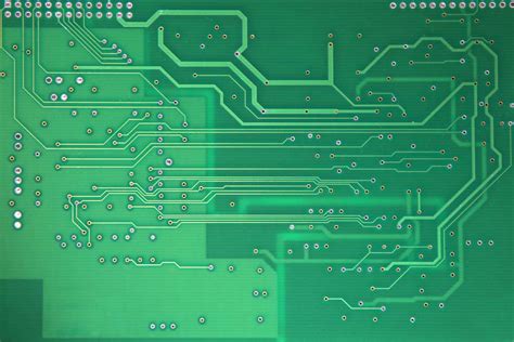
Printed Circuit Board (PCB) prototype design is a critical phase in the development of electronic devices, serving as a bridge between conceptualization and mass production. The process involves several essential steps, each contributing to the creation of a functional and reliable PCB. Understanding these steps is crucial for engineers and designers aiming to produce high-quality prototypes.
The initial step in PCB prototype design is the schematic capture.
This involves creating a detailed diagram that represents the electronic components and their interconnections. Using specialized software, designers can accurately depict the circuit, ensuring that all components are correctly placed and connected. This schematic serves as the blueprint for the subsequent stages of the design process.
Following the schematic capture, the next step is the component selection.
Choosing the right components is vital for the functionality and performance of the PCB. Designers must consider factors such as component availability, cost, and compatibility with the overall design. Additionally, it is essential to verify that the selected components meet the required specifications and standards.
Once the components are selected, the layout design begins.
This step involves arranging the components on the PCB and routing the electrical connections between them. The layout design must take into account various factors, including signal integrity, thermal management, and manufacturability. Proper placement of components and efficient routing of traces are crucial to minimize noise, interference, and potential signal degradation.
After completing the layout design, the next step is to perform a design rule check (DRC).
This automated process ensures that the PCB layout adheres to the predefined design rules and constraints. The DRC helps identify potential issues such as spacing violations, trace width errors, and other design flaws that could affect the performance and manufacturability of the PCB. Addressing these issues early in the design process can save time and resources in the long run.
Subsequently, the PCB prototype undergoes simulation and testing.
Simulation tools allow designers to analyze the behavior of the circuit under various conditions, identifying potential problems before physical prototyping. This step is crucial for verifying the functionality and performance of the design, ensuring that it meets the desired specifications. Testing the prototype in a controlled environment helps identify any discrepancies or issues that need to be addressed before moving forward.
Once the design is validated through simulation and testing, the next step is to generate the necessary manufacturing files.
These files, including Gerber files, drill files, and bill of materials (BOM), provide detailed instructions for fabricating the PCB. Accurate and comprehensive manufacturing files are essential for ensuring that the prototype is produced correctly and efficiently.
Finally, the PCB prototype is fabricated and assembled. This involves producing the physical board, populating it with the selected components, and soldering them in place. The assembly process must be carried out with precision to ensure that all components are correctly positioned and securely attached. Once assembled, the prototype undergoes further testing to verify its functionality and performance.
In conclusion, PCB prototype design is a multifaceted process that requires careful planning, attention to detail, and rigorous testing. Each step, from schematic capture to final assembly, plays a crucial role in ensuring the success of the prototype. By following these essential steps, designers can create reliable and high-quality PCB prototypes that pave the way for successful electronic products.
Common Mistakes To Avoid In PCB Prototyping
In the realm of electronics, PCB prototyping is a critical phase that can significantly influence the success of a project. However, even seasoned engineers can fall prey to common mistakes that can derail the process. One prevalent error is neglecting to thoroughly review the design specifications before commencing the prototyping phase. This oversight can lead to a cascade of issues, including incorrect component placement and routing errors, which can be costly and time-consuming to rectify. Therefore, it is imperative to meticulously verify all design parameters to ensure they align with the project requirements.
Another frequent mistake is inadequate attention to the layout of the PCB.
The layout is not merely a matter of placing components on a board; it involves strategic planning to optimize performance and minimize potential issues such as signal interference and thermal management problems. Poor layout decisions can result in signal integrity issues, which can compromise the functionality of the final product. To avoid this, designers should employ best practices such as maintaining proper spacing between components, using appropriate trace widths, and ensuring efficient grounding.
Furthermore, overlooking the importance of design for manufacturability (DFM) can lead to significant setbacks.
DFM considerations are crucial to ensure that the PCB can be produced efficiently and cost-effectively. Ignoring these aspects can result in boards that are difficult or impossible to manufacture, leading to delays and increased costs. It is essential to collaborate closely with the manufacturing team during the design phase to identify and address potential manufacturability issues early on.
Additionally, insufficient testing and validation of the prototype can be a critical pitfall.
Rushing through the testing phase or relying on limited testing scenarios can result in undetected flaws that may only become apparent during mass production or, worse, in the field. Comprehensive testing, including functional, environmental, and stress testing, is vital to ensure the prototype meets all performance and reliability standards. This thorough approach helps to identify and rectify issues before they escalate into more significant problems.
Moreover, failing to consider the thermal management of the PCB can lead to overheating and subsequent failure of the board.
Effective thermal management involves not only the placement of heat-generating components but also the incorporation of heat sinks, thermal vias, and appropriate materials to dissipate heat efficiently. Neglecting these aspects can result in reduced lifespan and reliability of the PCB, ultimately affecting the overall performance of the electronic device.
Another common mistake is underestimating the importance of documentation.
Comprehensive documentation is essential for both the design and manufacturing processes. It provides a clear roadmap for the production team and ensures that any future modifications or troubleshooting can be conducted efficiently. Inadequate documentation can lead to miscommunication, errors in production, and difficulties in maintaining or upgrading the PCB.
Lastly, ignoring the potential impact of electromagnetic interference (EMI) can be detrimental.
EMI can cause significant disruptions in the functionality of the PCB, leading to erratic behavior or complete failure. To mitigate EMI, designers should implement shielding techniques, use proper grounding methods, and carefully route high-frequency signals. Addressing EMI concerns during the design phase can prevent costly redesigns and ensure the reliability of the final product.
In conclusion, avoiding these common mistakes in PCB prototyping requires a meticulous and methodical approach. By thoroughly reviewing design specifications, optimizing layout, considering manufacturability, conducting comprehensive testing, managing thermal aspects, ensuring proper documentation, and addressing EMI concerns, designers can significantly enhance the success rate of their PCB prototypes. This proactive approach not only saves time and resources but also paves the way for the development of reliable and high-performing electronic devices.
Innovative Techniques For Rapid PCB Prototyping
In the realm of electronics, the demand for rapid and efficient PCB (Printed Circuit Board) prototyping has never been more critical. As technology advances at an unprecedented pace, the need for innovative techniques to expedite the prototyping process becomes paramount.
One such technique that has gained significant traction is the use of computer-aided design (CAD) software.
CAD tools have revolutionized the way engineers and designers approach PCB prototyping by enabling precise and intricate designs to be created with remarkable speed. These tools allow for the simulation of circuit behavior, which helps in identifying potential issues before the physical prototype is produced, thereby saving both time and resources.
Transitioning from design to physical production, another innovative technique that has emerged is the use of 3D printing technology.
3D printing has made it possible to create complex PCB prototypes with a high degree of accuracy. This method not only accelerates the prototyping process but also allows for greater flexibility in design modifications. By using conductive inks and substrates, 3D printers can produce functional circuit boards that can be tested and iterated upon rapidly. This approach is particularly beneficial for small-scale production runs and for projects that require quick turnaround times.
In addition to 3D printing, the advent of automated pick-and-place machines has further streamlined the PCB prototyping process.
These machines are capable of placing components onto the PCB with exceptional precision and speed. By automating this aspect of the assembly process, the likelihood of human error is significantly reduced, leading to higher quality prototypes. Moreover, the use of automated pick-and-place machines allows for the handling of increasingly smaller and more complex components, which is essential as electronic devices continue to miniaturize.
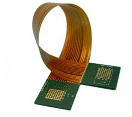
Furthermore, the integration of advanced materials has also played a crucial role in enhancing PCB prototyping techniques.
High-performance materials such as flexible substrates and advanced laminates have expanded the possibilities for PCB design. Flexible PCBs, for instance, can be bent and folded to fit into unconventional spaces, making them ideal for wearable technology and other compact devices. The use of advanced laminates, on the other hand, improves the thermal and electrical performance of the PCB, which is vital for high-frequency applications.
Another noteworthy technique is the implementation of Design for Manufacturability (DFM) principles.
DFM involves designing PCBs in a way that simplifies the manufacturing process and reduces potential issues during production. By considering factors such as component placement, trace routing, and thermal management during the design phase, engineers can create prototypes that are not only easier to manufacture but also more reliable. This proactive approach helps in minimizing costly revisions and accelerates the transition from prototype to final product.
Lastly, the utilization of rapid prototyping services offered by specialized companies has become increasingly popular.
These services provide access to state-of-the-art equipment and expertise, enabling designers to produce high-quality prototypes in a fraction of the time it would take using traditional methods. By outsourcing the prototyping process to these specialized firms, companies can focus on other critical aspects of product development, thereby enhancing overall efficiency.
In conclusion, the landscape of PCB prototyping has been transformed by a multitude of innovative techniques. From the use of CAD software and 3D printing to automated assembly and advanced materials, these advancements have significantly accelerated the prototyping process. By embracing these techniques, engineers and designers can bring their ideas to life more quickly and efficiently, ultimately driving innovation in the electronics industry.
Choosing The Right Materials For Your PCB Prototype
When embarking on the journey of PCB prototype design, one of the most critical decisions involves selecting the appropriate materials. The choice of materials can significantly impact the performance, reliability, and cost of the final product. Therefore, understanding the various options and their implications is essential for any designer aiming to create an effective and efficient PCB prototype.
To begin with, the substrate material forms the foundation of any PCB.
The most commonly used substrate is FR-4, a composite material made of woven fiberglass cloth with an epoxy resin binder that is flame resistant. FR-4 is favored for its excellent mechanical strength, electrical insulation properties, and cost-effectiveness. However, for applications requiring higher performance, such as high-frequency circuits or those exposed to extreme environmental conditions, alternative substrates like polyimide, PTFE (Teflon), or ceramic may be more suitable. These materials offer superior thermal stability, lower dielectric constants, and better signal integrity, albeit at a higher cost.
Transitioning to the conductive layers, copper is the material of choice due to its excellent electrical conductivity and relatively low cost.
The thickness of the copper layer, often referred to as copper weight, is a crucial parameter that influences the current-carrying capacity and thermal management of the PCB. Standard copper weights range from 1 oz/ft² to 3 oz/ft², but for high-power applications, thicker copper layers may be necessary. It is important to balance the copper weight with the overall design requirements to ensure optimal performance without unnecessary expense.
Next, the choice of solder mask material is another vital consideration.
The solder mask is a thin layer of polymer applied over the copper traces to prevent short circuits and protect against environmental damage. Epoxy liquid photoimageable (LPI) solder masks are widely used due to their excellent adhesion, chemical resistance, and ease of application. However, for PCBs that will be exposed to harsh conditions or require high reliability, such as in aerospace or medical devices, more robust materials like polyimide or liquid crystal polymer (LCP) may be preferred.
Furthermore, the selection of the surface finish is critical for ensuring good solderability and protecting the exposed copper from oxidation.
Common surface finishes include HASL (Hot Air Solder Leveling), ENIG (Electroless Nickel Immersion Gold), and OSP (Organic Solderability Preservative). HASL is cost-effective and provides good solderability but may not be suitable for fine-pitch components due to its uneven surface. ENIG offers a flat, smooth surface and excellent corrosion resistance, making it ideal for high-density and high-reliability applications, though it comes at a higher cost. OSP is an environmentally friendly option that provides a flat surface and good solderability but may not be as durable as other finishes.
In addition to these primary materials, other factors such as the choice of adhesives, laminates, and via fill materials can also influence the performance and manufacturability of the PCB prototype. Each material choice should be carefully evaluated in the context of the specific application requirements, including electrical performance, thermal management, mechanical strength, and environmental conditions.
In conclusion, selecting the right materials for your PCB prototype is a multifaceted process that requires a thorough understanding of the available options and their respective trade-offs. By carefully considering the substrate, conductive layers, solder mask, surface finish, and other ancillary materials, designers can ensure that their PCB prototypes meet the desired performance criteria while remaining cost-effective and reliable. This meticulous approach to material selection is fundamental to the success of any PCB design project.