Pcb pottery
History Of PCB Pottery: From Inception To Modern Day
The history of PCB pottery is a fascinating journey that traces its origins from humble beginnings to its current status as a celebrated art form.
The inception of PCB pottery can be traced back to ancient civilizations, where the need for functional and decorative items led to the development of various pottery techniques.
Early potters utilized locally available materials, such as clay and natural pigments, to create vessels and figurines that served both practical and ceremonial purposes. Over time, these early techniques evolved, influenced by cultural exchanges and technological advancements.
As societies progressed, so did the complexity and sophistication of pottery.
The introduction of the potter’s wheel around 3000 BCE marked a significant milestone in the history of pottery, allowing for more uniform and intricate designs. This innovation spread across different regions, each adapting the technique to their unique cultural contexts. In the case of PCB pottery, the integration of these advancements led to the creation of distinct styles that reflected the artistic sensibilities and functional needs of the communities that produced them.
The medieval period saw further refinement in pottery techniques, with the development of glazing methods that enhanced both the aesthetic appeal and durability of ceramic items.
During this time, PCB pottery began to gain recognition for its unique characteristics, such as intricate patterns and vibrant colors. The use of kilns allowed for more controlled firing processes, resulting in higher quality and more consistent products. This period also witnessed the establishment of pottery guilds, which played a crucial role in preserving and transmitting the knowledge and skills associated with the craft.
The Renaissance era brought about a renewed interest in classical art forms, including pottery.
PCB pottery, in particular, experienced a resurgence as artisans sought to revive and reinterpret traditional designs. This period was marked by a fusion of old and new techniques, leading to the creation of pieces that were both innovative and rooted in historical practices. The influence of trade and exploration also introduced new materials and ideas, further enriching the repertoire of PCB pottery.
The Industrial Revolution of the 18th and 19th centuries introduced mass production techniques that transformed the pottery industry.
While this shift allowed for the widespread availability of ceramic goods, it also posed challenges for traditional potters who relied on handcrafted methods. Despite these challenges, PCB pottery managed to retain its distinct identity, thanks in part to the efforts of dedicated artisans and cultural preservationists. The establishment of pottery schools and workshops helped to ensure the continuity of traditional techniques while also encouraging experimentation and innovation.
In the modern day, PCB pottery continues to thrive as both an art form and a functional craft.
Contemporary potters draw inspiration from historical practices while also incorporating modern materials and technologies. The global appreciation for handmade and artisanal goods has further bolstered the popularity of PCB pottery, with collectors and enthusiasts seeking out unique and high-quality pieces. Additionally, the rise of digital platforms has provided potters with new avenues for showcasing and selling their work, reaching audiences far beyond their local communities.
In conclusion, the history of PCB pottery is a testament to the enduring appeal and adaptability of this ancient craft. From its early beginnings to its present-day manifestations, PCB pottery has continually evolved, reflecting the changing needs and tastes of the societies that produce and appreciate it. Through the efforts of skilled artisans and the support of a global community, PCB pottery remains a vibrant and dynamic art form that continues to captivate and inspire.
Techniques And Tools Used In PCB Pottery Crafting
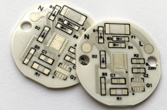
PCB pottery, a fascinating blend of traditional craftsmanship and modern technology, has emerged as a unique art form that captivates both artisans and tech enthusiasts alike. This innovative craft involves the creation of pottery using printed circuit boards (PCBs) as a primary material, resulting in pieces that are not only visually striking but also imbued with a sense of technological sophistication. To fully appreciate the intricacies of PCB pottery, it is essential to understand the techniques and tools employed in its crafting.
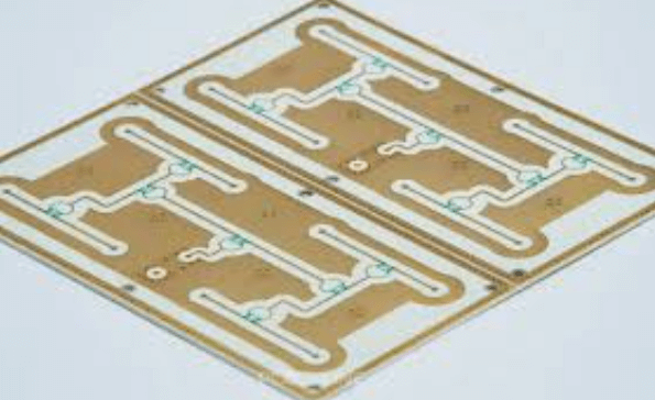
The process of creating PCB pottery begins with the selection of suitable PCBs.
These boards, typically discarded from electronic devices, are chosen based on their size, shape, and the intricacy of their circuitry patterns. The first step involves cleaning the PCBs to remove any residual solder, flux, or other contaminants. This is usually done using a combination of isopropyl alcohol and a soft brush, ensuring that the boards are free from any impurities that could affect the final product.
Once the PCBs are cleaned, they are cut into the desired shapes using precision tools such as laser cutters or CNC machines.
These tools allow for intricate designs and precise cuts, which are crucial for the aesthetic appeal of the final pottery piece. The cut PCBs are then arranged and layered to form the basic structure of the pottery. This layering technique not only adds depth and complexity to the design but also enhances the structural integrity of the piece.
To bind the layers of PCBs together, a specialized adhesive is used.
This adhesive must be strong enough to hold the layers securely while also being flexible enough to accommodate any slight movements or adjustments during the crafting process. Epoxy resin is commonly used for this purpose, as it provides a durable and transparent bond that does not detract from the visual appeal of the PCBs.
After the basic structure is assembled, the next step involves shaping and refining the pottery.
This is done using a combination of traditional pottery tools and modern equipment. For instance, potter’s wheels can be adapted to accommodate the unique properties of PCB materials, allowing artisans to shape the pottery with precision and control. Additionally, sanding and polishing tools are used to smooth out any rough edges and enhance the overall finish of the piece.
One of the most distinctive aspects of PCB pottery is the incorporation of electronic components into the design.
These components, such as resistors, capacitors, and LEDs, are carefully selected and strategically placed to enhance the visual and functional aspects of the pottery. For example, LEDs can be embedded within the layers of PCBs to create stunning lighting effects, adding an element of interactivity to the piece.
The final step in the crafting process is the application of a protective coating. This coating serves multiple purposes: it protects the PCBs from environmental factors such as moisture and dust, enhances the durability of the pottery, and provides a glossy finish that highlights the intricate circuitry patterns. Polyurethane or acrylic coatings are commonly used for this purpose, as they offer excellent protection and a high-quality finish.
In conclusion, the techniques and tools used in PCB pottery crafting are a testament to the ingenuity and creativity of modern artisans. By combining traditional pottery methods with advanced technological processes, they have created a unique art form that bridges the gap between the past and the future. The result is a collection of pottery pieces that are not only beautiful and functional but also a celebration of the harmonious coexistence of art and technology.
The Environmental Impact Of PCB Pottery Production
The production of PCB pottery, while innovative and aesthetically appealing, carries significant environmental implications that merit close examination. Printed Circuit Board (PCB) pottery involves the integration of electronic waste into ceramic art, transforming discarded circuit boards into unique, decorative pieces. This practice, although creative, raises several environmental concerns that need to be addressed to ensure sustainable production methods.
To begin with, the extraction and processing of raw materials for PCBs are resource-intensive activities that contribute to environmental degradation.
The manufacturing of PCBs involves the use of various metals such as copper, gold, and silver, which are mined from the earth. Mining operations often lead to deforestation, soil erosion, and contamination of water sources due to the release of toxic chemicals. Consequently, the initial stages of PCB production already set a precedent for environmental harm, which is further compounded when these materials are repurposed for pottery.
Moreover, the disposal of electronic waste, or e-waste, poses a significant environmental challenge.
E-waste contains hazardous substances such as lead, mercury, and cadmium, which can leach into the soil and water, causing pollution and health risks to humans and wildlife. By incorporating e-waste into pottery, there is a potential risk of these toxic elements being released during the production process. For instance, the firing of ceramics at high temperatures could potentially volatilize harmful substances, leading to air pollution and occupational health hazards for artisans.
In addition to the direct environmental impacts, the energy consumption associated with PCB pottery production is another critical factor to consider.
The process of creating ceramic pieces involves high-temperature kilns that consume substantial amounts of energy, often derived from non-renewable sources such as coal and natural gas. This reliance on fossil fuels contributes to greenhouse gas emissions, exacerbating climate change. Therefore, the energy-intensive nature of ceramic production, combined with the environmental footprint of PCB manufacturing, underscores the need for more sustainable practices in this artistic endeavor.
Transitioning to more sustainable methods of PCB pottery production requires a multifaceted approach.
One potential solution is the adoption of cleaner energy sources for firing kilns, such as solar or wind power. By reducing reliance on fossil fuels, the carbon footprint of the production process can be significantly minimized. Additionally, implementing stringent safety protocols to manage and mitigate the release of toxic substances during the production process is crucial. This could involve the use of advanced filtration systems and protective equipment for artisans to ensure a safer working environment.
Furthermore, promoting the recycling and proper disposal of e-waste can help mitigate the environmental impact of PCB pottery.
Encouraging the collection and recycling of electronic components before they reach landfills can reduce the amount of hazardous waste entering the environment. Collaborating with e-waste recycling programs and organizations can provide a steady supply of materials for PCB pottery while ensuring that harmful substances are appropriately managed.
In conclusion, while PCB pottery represents a fascinating intersection of technology and art, it is imperative to address the environmental ramifications associated with its production. By adopting sustainable practices, utilizing cleaner energy sources, and promoting responsible e-waste management, the environmental impact of PCB pottery can be significantly reduced. This approach not only preserves the integrity of the environment but also ensures the longevity and ethical viability of this innovative art form.

Innovative Designs And Trends In PCB Pottery
In recent years, the intersection of technology and traditional craftsmanship has given rise to innovative designs and trends in PCB pottery. This unique fusion of printed circuit boards (PCBs) and ceramic art has captivated the attention of both tech enthusiasts and art connoisseurs alike. As we delve into this fascinating domain, it becomes evident that PCB pottery is not merely a fleeting trend but a burgeoning field that holds significant potential for future artistic and technological advancements.
To begin with, the concept of PCB pottery involves embedding electronic components within ceramic materials, thereby creating functional and aesthetically pleasing objects.
This amalgamation of electronics and ceramics is achieved through meticulous design and engineering processes. Artists and engineers collaborate to ensure that the electronic components are seamlessly integrated into the ceramic structure without compromising the integrity or beauty of the piece. Consequently, the resulting creations are not only visually striking but also possess practical applications, such as interactive art installations, smart home decor, and even wearable technology.
One of the most notable trends in PCB pottery is the use of advanced manufacturing techniques to produce intricate and detailed designs.
For instance, 3D printing technology has revolutionized the way ceramic objects are created, allowing for greater precision and complexity in design. By utilizing 3D printers, artists can experiment with various shapes, patterns, and textures that would be challenging to achieve through traditional pottery methods. Moreover, the integration of PCBs into these 3D-printed ceramics opens up a myriad of possibilities for interactive and responsive art pieces.
In addition to 3D printing, another significant trend in PCB pottery is the exploration of sustainable and eco-friendly materials.
As environmental concerns continue to rise, artists and engineers are increasingly seeking ways to minimize the ecological impact of their creations. This has led to the development of biodegradable PCBs and the use of recycled ceramic materials. By adopting sustainable practices, the field of PCB pottery not only contributes to the reduction of electronic waste but also promotes a more environmentally conscious approach to art and technology.
Furthermore, the aesthetic appeal of PCB pottery is enhanced by the incorporation of various artistic styles and cultural influences.
Artists draw inspiration from diverse sources, ranging from traditional pottery techniques to contemporary digital art. This eclectic mix of influences results in a rich tapestry of designs that reflect both the heritage of ceramic art and the cutting-edge nature of modern technology. For example, some artists may incorporate intricate patterns reminiscent of ancient pottery, while others may experiment with minimalist and abstract designs that emphasize the electronic components.
As we look to the future, it is clear that the potential applications of PCB pottery are vast and varied.
Beyond the realm of art and decor, this innovative field holds promise for advancements in areas such as medical devices, educational tools, and even space exploration. The ability to embed electronic functionality within durable and heat-resistant ceramic materials opens up new possibilities for creating robust and versatile devices that can withstand extreme conditions.
In conclusion, the innovative designs and trends in PCB pottery represent a harmonious blend of technology and artistry. Through the use of advanced manufacturing techniques, sustainable materials, and diverse artistic influences, this emerging field continues to push the boundaries of what is possible in both the art and technology sectors. As artists and engineers continue to collaborate and experiment, we can expect to see even more groundbreaking creations that challenge our perceptions and inspire future innovations.