Pcb multilayer stack up
Benefits Of Multilayer PCB Stack Up In Modern Electronics
In the rapidly evolving landscape of modern electronics, the demand for more compact, efficient, and high-performance devices has never been greater.
One of the key innovations that have enabled this progress is the multilayer printed circuit board (PCB) stack-up.
This sophisticated technology offers numerous benefits that are crucial for the development and functionality of contemporary electronic devices.
To begin with, multilayer PCB stack-ups significantly enhance the electrical performance of electronic circuits.
By incorporating multiple layers of conductive material separated by insulating layers, these PCBs can support more complex and higher-density circuits. This is particularly advantageous for applications requiring high-speed signal transmission and reduced electromagnetic interference (EMI). The ability to strategically place ground and power planes within the stack-up helps to minimize signal noise and crosstalk, thereby ensuring more reliable and efficient operation of the electronic device.
Moreover, the compact nature of multilayer PCBs is a substantial benefit in the design of modern electronics.
As devices become smaller and more portable, the need to fit more functionality into a limited space becomes paramount. Multilayer PCBs allow for the integration of more components and interconnections within a smaller footprint, which is essential for the miniaturization of devices such as smartphones, tablets, and wearable technology. This compactness does not come at the expense of performance; rather, it often enhances it by reducing the length of interconnections and thus the potential for signal degradation.
In addition to improved performance and compactness, multilayer PCB stack-ups offer greater design flexibility.
Designers can create more intricate and sophisticated circuit layouts by utilizing multiple layers. This flexibility is particularly beneficial in the development of advanced technologies such as artificial intelligence, Internet of Things (IoT) devices, and high-frequency communication systems. The ability to customize the stack-up configuration to meet specific design requirements allows for optimized performance tailored to the unique needs of each application.
Furthermore, the reliability and durability of multilayer PCBs are noteworthy advantages.
The use of multiple layers and high-quality materials enhances the structural integrity of the board, making it more resistant to environmental stresses such as temperature fluctuations, humidity, and mechanical shocks. This robustness is critical for applications in harsh environments, including automotive, aerospace, and industrial sectors, where electronic devices must perform consistently under challenging conditions.
Another significant benefit of multilayer PCB stack-ups is their contribution to cost efficiency in the long run.
While the initial manufacturing process may be more complex and costly compared to single-layer or double-layer PCBs, the overall cost savings become apparent when considering the enhanced performance, reduced need for additional components, and lower failure rates. The ability to integrate more functionality into a single board reduces the need for multiple PCBs and interconnections, thereby simplifying assembly processes and reducing production costs.
In conclusion, the benefits of multilayer PCB stack-ups in modern electronics are manifold. They offer superior electrical performance, compactness, design flexibility, reliability, and cost efficiency, all of which are essential for meeting the demands of today’s advanced electronic devices. As technology continues to advance, the role of multilayer PCBs will undoubtedly remain pivotal in driving innovation and enabling the development of increasingly sophisticated and high-performing electronic systems.
Key Considerations For Designing A Multilayer PCB Stack Up
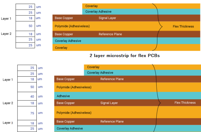
Designing a multilayer PCB stack-up is a complex process that requires careful consideration of various factors to ensure optimal performance and reliability. One of the primary considerations is the number of layers required. This decision is influenced by the complexity of the circuit, the need for signal integrity, and the space constraints of the final product. Typically, more layers allow for better separation of power and ground planes, which can significantly reduce electromagnetic interference (EMI) and improve signal integrity.
Another critical factor is the selection of materials.
The dielectric material between the layers plays a crucial role in determining the electrical performance of the PCB. Materials with low dielectric constants are preferred for high-frequency applications as they reduce signal loss. Additionally, the thermal properties of the materials must be considered, especially for applications that involve high power or operate in harsh environments. The choice of materials also impacts the overall cost of the PCB, making it essential to balance performance requirements with budget constraints.
The arrangement of layers, or the stack-up configuration, is another vital aspect.
A well-designed stack-up can minimize crosstalk and EMI while ensuring signal integrity. Typically, a symmetrical stack-up is preferred to prevent warping during the manufacturing process. For instance, a common four-layer stack-up might include a signal layer, a ground plane, a power plane, and another signal layer. This configuration helps to isolate the signal layers from each other, reducing interference and improving performance.
Impedance control is another key consideration in multilayer PCB design.
Impedance mismatches can lead to signal reflections, which degrade signal quality and can cause data errors. To achieve controlled impedance, the width of the traces and the thickness of the dielectric material must be precisely calculated. This often requires close collaboration with the PCB manufacturer to ensure that the design specifications can be met during production.
Thermal management is also a crucial aspect of multilayer PCB design.
As electronic components become more powerful and compact, the heat generated can significantly impact the performance and longevity of the PCB. Effective thermal management strategies, such as the use of thermal vias and heat sinks, must be incorporated into the design to dissipate heat efficiently. Additionally, the placement of components should be carefully planned to avoid hotspots and ensure even heat distribution.
The manufacturability of the PCB is another important consideration.
Complex multilayer designs can be challenging to produce, and certain design choices can complicate the manufacturing process. For example, very thin or very thick PCBs can be difficult to handle and may require specialized equipment. Therefore, it is essential to work closely with the manufacturer during the design phase to ensure that the PCB can be produced reliably and cost-effectively.
Finally, testing and validation are critical steps in the design process.
Prototyping and rigorous testing can help identify potential issues early, allowing for adjustments before full-scale production. This can save time and resources in the long run, ensuring that the final product meets all performance and reliability requirements.
In conclusion, designing a multilayer PCB stack-up involves a careful balance of various factors, including the number of layers, material selection, stack-up configuration, impedance control, thermal management, manufacturability, and thorough testing. By considering these key aspects, designers can create high-performance, reliable PCBs that meet the demands of modern electronic applications.
Common Challenges In Multilayer PCB Stack Up And How To Overcome Them
Multilayer PCB stack-up design is a critical aspect of modern electronics, enabling the integration of complex circuits within compact spaces. However, this intricate process is fraught with challenges that can impact the performance, reliability, and manufacturability of the final product.
One of the most common challenges in multilayer PCB stack-up is signal integrity.
As the number of layers increases, so does the complexity of maintaining signal integrity. High-speed signals are particularly susceptible to issues such as crosstalk, impedance mismatches, and signal reflection. To overcome these challenges, designers must carefully plan the layer arrangement, ensuring that signal layers are adequately separated by ground or power planes. This not only minimizes crosstalk but also provides a controlled impedance environment, essential for high-speed signal transmission.
Another significant challenge is thermal management.
Multilayer PCBs, especially those used in high-power applications, can generate substantial heat. Effective thermal management is crucial to prevent overheating and ensure the longevity of the components. One approach to address this issue is to incorporate thermal vias, which help dissipate heat from the inner layers to the outer layers. Additionally, using materials with high thermal conductivity and designing for optimal airflow can further enhance thermal performance.
Manufacturability is also a critical concern in multilayer PCB stack-up design.
As the number of layers increases, so does the complexity of the manufacturing process. Issues such as layer misalignment, warping, and delamination can arise, leading to increased production costs and reduced yield. To mitigate these risks, it is essential to work closely with the PCB manufacturer during the design phase. This collaboration ensures that the design is optimized for the specific manufacturing capabilities and limitations, reducing the likelihood of defects and improving overall yield.
Furthermore, the choice of materials plays a pivotal role in multilayer PCB stack-up design.
Different materials have varying dielectric constants, thermal properties, and mechanical strengths, all of which can impact the performance and reliability of the PCB. Selecting the appropriate materials requires a thorough understanding of the application’s requirements and the trade-offs involved. For instance, while high-frequency applications may benefit from materials with low dielectric constants, these materials may also be more expensive or challenging to work with. Balancing these factors is crucial to achieving a cost-effective and high-performance design.
In addition to these technical challenges, designers must also consider the impact of regulatory and industry standards.
Compliance with standards such as IPC-2221 (Generic Standard on Printed Board Design) and IPC-6012 (Qualification and Performance Specification for Rigid Printed Boards) is essential to ensure the quality and reliability of the PCB. Adhering to these standards can also facilitate smoother communication and collaboration with manufacturers and other stakeholders.
In conclusion, multilayer PCB stack-up design presents a myriad of challenges, ranging from signal integrity and thermal management to manufacturability and material selection. However, by adopting a systematic and collaborative approach, these challenges can be effectively addressed. Careful planning, close collaboration with manufacturers, and a thorough understanding of material properties and industry standards are key to overcoming these obstacles and achieving a successful multilayer PCB design. As technology continues to advance, the ability to navigate these complexities will be increasingly vital, ensuring that multilayer PCBs can meet the ever-growing demands of modern electronic applications.

Innovations In Multilayer PCB Stack Up Technology
The evolution of multilayer PCB stack-up technology has been a cornerstone in the advancement of modern electronics, driving innovations across various industries. As electronic devices become increasingly complex and compact, the demand for sophisticated multilayer PCB designs has surged. This has led to significant advancements in materials, fabrication techniques, and design methodologies, all aimed at enhancing the performance, reliability, and functionality of multilayer PCBs.
One of the most notable innovations in multilayer PCB stack-up technology is the development of advanced materials.
Traditional materials such as FR-4 have been the industry standard for many years; however, the limitations of these materials in high-frequency and high-speed applications have prompted the exploration of alternatives. High-performance materials like polyimide, Rogers, and Teflon have emerged, offering superior thermal stability, dielectric properties, and signal integrity. These materials are particularly beneficial in applications such as aerospace, telecommunications, and high-frequency RF circuits, where performance and reliability are paramount.
In addition to material advancements, fabrication techniques have also seen significant improvements.
The advent of laser drilling technology, for instance, has revolutionized the way vias are created in multilayer PCBs. Laser drilling allows for the creation of microvias, which are much smaller than traditional mechanical vias. This not only enables higher component density but also improves signal integrity by reducing the parasitic inductance and capacitance associated with larger vias. Furthermore, the use of sequential lamination processes has allowed for the construction of complex multilayer boards with multiple buried and blind vias, enhancing the overall design flexibility.
Another critical innovation in multilayer PCB stack-up technology is the implementation of advanced design methodologies.
The integration of computer-aided design (CAD) tools and simulation software has streamlined the design process, enabling engineers to create more intricate and optimized PCB layouts. These tools allow for precise control over layer stack-up configurations, impedance matching, and signal routing, ensuring that the final product meets the stringent performance requirements of modern electronic devices. Additionally, the use of design for manufacturability (DFM) principles has become increasingly important, as it helps to minimize production costs and reduce the likelihood of manufacturing defects.
The push towards miniaturization and higher performance has also led to the adoption of embedded component technology in multilayer PCBs.
By embedding passive and active components within the PCB layers, designers can achieve significant space savings and improve electrical performance. This approach is particularly advantageous in applications where space is at a premium, such as in wearable devices, medical implants, and advanced computing systems. Moreover, the integration of embedded components can enhance thermal management by distributing heat more evenly across the PCB, thereby improving the overall reliability of the device.
As the demand for more advanced electronic devices continues to grow, the importance of innovations in multilayer PCB stack-up technology cannot be overstated.
The ongoing advancements in materials, fabrication techniques, and design methodologies are driving the development of more powerful, reliable, and compact electronic systems. These innovations are not only enabling the creation of cutting-edge consumer electronics but are also paving the way for breakthroughs in various high-tech industries. As we look to the future, it is clear that the continued evolution of multilayer PCB stack-up technology will play a crucial role in shaping the next generation of electronic devices.