Pcb manufacturing training
Understanding The Basics Of PCB Design And Layout
Printed Circuit Board (PCB) manufacturing is a critical aspect of modern electronics, serving as the backbone for virtually all electronic devices. Understanding the basics of PCB design and layout is essential for anyone involved in electronics engineering or manufacturing. This knowledge not only ensures the functionality and reliability of electronic devices but also optimizes their performance and cost-effectiveness.
To begin with, PCB design involves creating a schematic diagram that represents the electronic circuit.
This schematic is a blueprint that outlines the connections between various electronic components such as resistors, capacitors, and integrated circuits. The design process starts with selecting the appropriate components and defining their electrical connections. This step is crucial as it lays the foundation for the subsequent layout process. A well-designed schematic ensures that the circuit will function as intended and helps in identifying potential issues early in the design phase.
Once the schematic is complete, the next step is the PCB layout.
This involves placing the components on the board and routing the electrical connections between them. The layout process requires careful consideration of several factors, including the physical size of the components, the available board space, and the electrical characteristics of the circuit. Proper component placement is vital to minimize signal interference and ensure efficient heat dissipation. Additionally, the routing of electrical connections, or traces, must be done in a way that minimizes resistance and inductance, which can affect the circuit’s performance.
Transitioning from design to layout, it is important to consider the type of PCB being used.
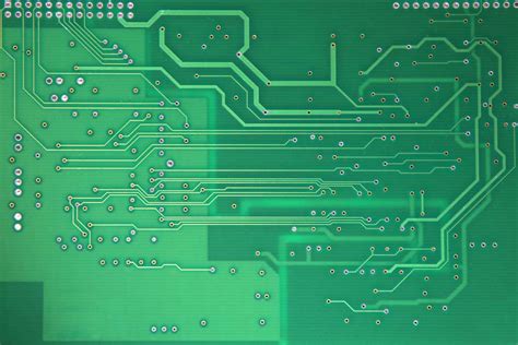
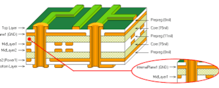
There are various types of PCBs, including single-sided, double-sided, and multi-layer boards. Single-sided PCBs have components and traces on one side of the board, making them simpler and cheaper to manufacture. Double-sided PCBs have components and traces on both sides, allowing for more complex circuits. Multi-layer PCBs have multiple layers of traces separated by insulating material, enabling even more complex and compact designs. The choice of PCB type depends on the complexity of the circuit and the specific requirements of the application.
Another critical aspect of PCB design and layout is the consideration of signal integrity.
Signal integrity refers to the quality of the electrical signals as they travel through the PCB. Poor signal integrity can lead to issues such as signal degradation, noise, and electromagnetic interference (EMI). To ensure good signal integrity, designers must follow best practices such as maintaining proper trace width and spacing, using ground planes, and minimizing the length of high-speed signal traces. Additionally, the use of decoupling capacitors can help to stabilize the power supply and reduce noise.
Thermal management is also a key consideration in PCB design and layout.
Electronic components generate heat during operation, and excessive heat can lead to component failure and reduced reliability. Effective thermal management involves designing the PCB layout to facilitate heat dissipation. This can be achieved through the use of thermal vias, heat sinks, and proper component placement. Ensuring adequate airflow around the PCB can also help to dissipate heat and maintain optimal operating temperatures.
In conclusion, understanding the basics of PCB design and layout is fundamental for the successful manufacturing of electronic devices. From creating a schematic diagram to considering signal integrity and thermal management, each step in the process plays a crucial role in ensuring the functionality and reliability of the final product. By adhering to best practices and considering the specific requirements of the application, designers can create efficient and cost-effective PCBs that meet the demands of modern electronics.
Essential Tools And Software For PCB Manufacturing
Printed Circuit Board (PCB) manufacturing is a complex process that requires a combination of specialized tools and software to ensure precision and efficiency. For those entering the field, understanding the essential tools and software is crucial for successful PCB design and production. This article aims to provide an overview of the key instruments and applications necessary for PCB manufacturing.
To begin with, the foundation of any PCB manufacturing process is the design phase, which heavily relies on Computer-Aided Design (CAD) software.
CAD tools such as Altium Designer, Eagle, and KiCad are indispensable for creating detailed schematics and layout designs. These software applications offer a range of features, including component libraries, routing tools, and simulation capabilities, which facilitate the creation of accurate and functional PCB designs. Transitioning from design to production, these CAD tools also generate Gerber files, which are the standard format for PCB manufacturing.
Once the design is finalized, the next step involves the use of photoplotters.
Photoplotters are essential for transferring the PCB design onto a photomask, which is then used to create the physical board. These devices use laser or LED technology to produce high-resolution images of the PCB layers on a photosensitive film. The precision of photoplotters ensures that even the smallest details of the design are accurately captured, which is critical for the subsequent etching process.
Following the creation of the photomask, the PCB material, typically a copper-clad laminate, undergoes a series of chemical processes.
Etching tanks and chemical baths are vital tools in this stage. Etching tanks contain etching solutions, such as ferric chloride or ammonium persulfate, which remove unwanted copper from the board, leaving only the desired circuit pattern. Proper handling and maintenance of these chemical baths are essential to ensure consistent results and to prevent contamination.
In addition to chemical processes, mechanical tools play a significant role in PCB manufacturing.
Drilling machines equipped with high-speed spindles are used to create precise holes for component leads and vias. These machines must be capable of drilling extremely small holes with high accuracy, as even minor deviations can affect the performance of the final product. Furthermore, CNC (Computer Numerical Control) milling machines are employed to cut the PCB to its final shape and to create any necessary slots or cutouts.
As the PCB takes shape, inspection and testing tools become crucial.
Optical inspection systems, such as Automated Optical Inspection (AOI) machines, are used to verify the integrity of the PCB by scanning for defects such as open circuits, short circuits, and misaligned components. These systems use advanced imaging technology to detect even the smallest imperfections, ensuring that only high-quality boards proceed to the next stage.
Finally, software tools for simulation and testing, such as SPICE (Simulation Program with Integrated Circuit Emphasis), are essential for validating the electrical performance of the PCB design. These tools allow engineers to simulate the behavior of the circuit under various conditions, identifying potential issues before the board is physically produced. This not only saves time and resources but also enhances the reliability of the final product.
In conclusion, PCB manufacturing is a multifaceted process that requires a combination of specialized tools and software. From CAD applications for design to photoplotters, etching tanks, drilling machines, and inspection systems, each tool plays a critical role in ensuring the precision and quality of the final product. Understanding and mastering these essential tools and software is fundamental for anyone aspiring to excel in the field of PCB manufacturing.
Common Mistakes To Avoid In PCB Fabrication
In the realm of PCB manufacturing training, understanding common mistakes to avoid in PCB fabrication is crucial for ensuring high-quality outcomes. One of the most frequent errors encountered is improper design layout. A well-thought-out design is the foundation of a successful PCB, and neglecting this step can lead to numerous issues down the line. For instance, inadequate spacing between components can cause short circuits, while poor placement of vias can result in signal integrity problems. Therefore, it is essential to adhere to design guidelines and utilize design rule checks (DRCs) to identify potential issues early in the process.
Another prevalent mistake is the selection of inappropriate materials.
The choice of substrate, copper thickness, and solder mask can significantly impact the performance and reliability of the PCB. Using materials that do not match the operational requirements of the device can lead to thermal management issues, mechanical failures, and even complete malfunction. Consequently, it is imperative to thoroughly understand the material properties and ensure they align with the intended application of the PCB.
Transitioning to the manufacturing process itself, one must be vigilant about the accuracy of the drilling process.
Misaligned or incorrectly sized holes can cause connectivity issues and impede the assembly process. Precision in drilling is paramount, and employing advanced drilling techniques and equipment can mitigate these risks. Additionally, regular maintenance and calibration of drilling machinery are necessary to maintain high standards of accuracy.
Furthermore, soldering errors are a common pitfall in PCB fabrication.
Cold solder joints, solder bridges, and insufficient solder can all compromise the functionality of the PCB. To avoid these issues, it is essential to maintain proper soldering temperatures and techniques. Automated soldering processes, such as reflow soldering, can enhance consistency and reduce the likelihood of human error. However, even automated processes require careful monitoring and quality control to ensure optimal results.
Another critical aspect to consider is the cleanliness of the PCB during and after fabrication.
Contaminants such as dust, oils, and residues can adversely affect the performance and reliability of the PCB. Implementing stringent cleaning protocols and using appropriate cleaning agents can help mitigate this risk. Additionally, ensuring a clean working environment and handling PCBs with care can prevent contamination.
Moreover, neglecting to perform thorough testing and inspection can lead to undetected defects and failures in the final product.
Electrical testing, such as continuity and isolation tests, can identify issues with connectivity and signal integrity. Visual inspections, both manual and automated, can detect physical defects such as misaligned components and soldering errors. Implementing a robust testing and inspection regimen is essential for ensuring the quality and reliability of the PCB.
Lastly, inadequate documentation and communication can lead to misunderstandings and errors throughout the fabrication process.
Clear and detailed documentation of design specifications, material requirements, and process parameters is vital for ensuring that all stakeholders are on the same page. Effective communication between design engineers, manufacturing personnel, and quality control teams can help identify and address potential issues before they escalate.
In conclusion, avoiding common mistakes in PCB fabrication requires a comprehensive understanding of the design, material selection, manufacturing processes, and quality control measures. By adhering to best practices and maintaining a vigilant approach, one can significantly enhance the quality and reliability of PCBs, ultimately leading to more successful and dependable electronic devices.
Advanced Techniques In PCB Prototyping And Testing
In the realm of PCB manufacturing, the transition from basic to advanced techniques in prototyping and testing is pivotal for ensuring the reliability and functionality of electronic devices. As technology continues to evolve, the demand for more sophisticated and efficient methods in PCB prototyping and testing has become increasingly critical. This necessitates a comprehensive understanding of advanced techniques that can significantly enhance the quality and performance of printed circuit boards.
One of the foremost advanced techniques in PCB prototyping is the utilization of high-density interconnect (HDI) technology.
HDI PCBs are characterized by their higher wiring density per unit area compared to traditional PCBs. This is achieved through the use of microvias, blind vias, and buried vias, which allow for more complex routing and greater component density. The implementation of HDI technology not only reduces the size and weight of the PCB but also improves signal integrity and overall performance. Consequently, mastering HDI techniques is essential for engineers aiming to produce cutting-edge electronic devices.
In addition to HDI technology, the adoption of flexible and rigid-flex PCBs represents another advanced prototyping technique.
Flexible PCBs are designed to bend and flex, making them ideal for applications where space constraints and mechanical stress are significant considerations. Rigid-flex PCBs combine the benefits of both rigid and flexible circuits, offering enhanced durability and reliability. These advanced PCB types require specialized design and manufacturing processes, including precise material selection and intricate layering techniques. As such, proficiency in flexible and rigid-flex PCB prototyping is indispensable for engineers working on innovative and compact electronic solutions.
Transitioning from prototyping to testing, advanced techniques in PCB testing are equally crucial for ensuring the functionality and longevity of the final product.
One such technique is automated optical inspection (AOI), which employs high-resolution cameras and sophisticated algorithms to detect defects in PCBs. AOI systems can identify issues such as solder joint defects, component misalignment, and surface contamination with remarkable accuracy and speed. By integrating AOI into the testing process, manufacturers can significantly reduce the likelihood of defective PCBs reaching the market, thereby enhancing product quality and customer satisfaction.
Another critical testing technique is in-circuit testing (ICT), which involves the use of a bed-of-nails tester to electrically probe the PCB and verify the functionality of individual components and connections.
ICT is highly effective in identifying manufacturing defects such as open circuits, short circuits, and incorrect component values. This method provides a comprehensive assessment of the PCB’s electrical performance, ensuring that any issues are promptly addressed before mass production. Mastery of ICT is essential for engineers seeking to deliver reliable and high-performance electronic products.
Moreover, advanced thermal testing techniques, such as thermal imaging and thermal cycling, play a vital role in assessing the thermal performance and durability of PCBs.
Thermal imaging allows engineers to visualize temperature distribution across the PCB, identifying hotspots and potential thermal management issues. Thermal cycling, on the other hand, subjects the PCB to repeated temperature fluctuations to evaluate its resistance to thermal stress. These techniques are indispensable for ensuring that PCBs can withstand the thermal demands of their intended applications, thereby enhancing their reliability and lifespan.
In conclusion, the mastery of advanced techniques in PCB prototyping and testing is fundamental for engineers striving to produce high-quality and reliable electronic devices. From HDI and flexible PCBs to AOI, ICT, and thermal testing, these sophisticated methods are essential for addressing the complexities of modern PCB manufacturing. By embracing these advanced techniques, engineers can ensure that their PCBs meet the stringent demands of today’s technology-driven world, ultimately contributing to the advancement of the electronics industry.