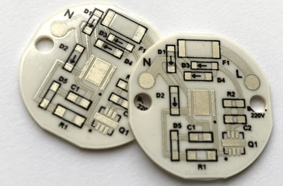
Pcb layouting
Best Practices For PCB Layouting Design
Printed Circuit Board (PCB) layout design is a critical aspect of electronics engineering, requiring meticulous attention to detail and adherence to best practices to ensure optimal performance and reliability.
One of the fundamental principles in PCB layout design is to start with a clear and well-organized schematic.
This schematic serves as the blueprint for the entire design process, providing a visual representation of the circuit and its components. By ensuring that the schematic is accurate and comprehensive, designers can avoid potential issues that may arise during the layout phase.
Transitioning from the schematic to the actual layout, it is essential to consider the placement of components.
Strategic component placement can significantly impact the performance of the PCB. For instance, placing components that interact frequently close to each other can minimize signal path lengths, thereby reducing potential signal integrity issues. Additionally, grouping components by function can simplify routing and enhance the overall organization of the board. It is also advisable to place critical components, such as microcontrollers and power regulators, in central locations to facilitate efficient power distribution and signal routing.
Another crucial aspect of PCB layout design is the management of signal integrity.
High-speed signals, in particular, require careful attention to avoid issues such as crosstalk and electromagnetic interference (EMI). To mitigate these risks, designers should use controlled impedance traces and maintain consistent trace widths and spacing. Furthermore, incorporating ground planes and power planes can provide a stable reference for signals and help dissipate heat, thereby improving the overall performance and reliability of the PCB.
Thermal management is another key consideration in PCB layout design.
As electronic components generate heat during operation, effective thermal management is essential to prevent overheating and ensure the longevity of the board. Designers can employ various techniques to manage heat, such as using thermal vias to transfer heat from the surface to internal layers, incorporating heat sinks, and optimizing the placement of heat-generating components. Additionally, maintaining adequate spacing between components can facilitate airflow and enhance heat dissipation.
Transitioning to the topic of routing, it is important to follow best practices to ensure efficient and reliable signal transmission.
One such practice is to use short and direct routing paths whenever possible, as longer paths can introduce signal delays and potential interference. Additionally, designers should avoid sharp angles in trace routing, as these can cause signal reflections and degrade signal quality. Instead, using smooth, curved traces can help maintain signal integrity. It is also beneficial to route differential pairs together, maintaining consistent spacing and length to ensure balanced signal transmission.
Power distribution is another critical element in PCB layout design. Ensuring that all components receive stable and adequate power is essential for the proper functioning of the board.
Designers should use wide traces for power and ground connections to minimize voltage drops and reduce resistance. Additionally, incorporating decoupling capacitors near power pins can help filter out noise and provide a stable power supply to sensitive components.
In conclusion, adhering to best practices in PCB layout design is essential for creating reliable and high-performance electronic devices. By starting with a well-organized schematic, strategically placing components, managing signal integrity, addressing thermal management, following efficient routing practices, and ensuring robust power distribution, designers can optimize their PCB layouts and achieve successful outcomes. These practices not only enhance the functionality and reliability of the PCB but also contribute to the overall success of the electronic product.
Common Mistakes In PCB Layout And How To Avoid Them
Printed Circuit Board (PCB) layouting is a critical step in the design and manufacturing of electronic devices. However, even experienced designers can fall prey to common mistakes that can compromise the functionality, reliability, and manufacturability of the final product. Understanding these pitfalls and learning how to avoid them is essential for producing high-quality PCBs.
One frequent mistake in PCB layouting is inadequate component placement.
Poorly placed components can lead to a host of issues, including signal integrity problems, increased electromagnetic interference (EMI), and difficulties in assembly. To avoid this, designers should prioritize placing components in a logical and efficient manner. High-speed components should be placed as close to each other as possible to minimize trace lengths, while power and ground planes should be strategically positioned to ensure proper power distribution and signal return paths.
Another common error is the improper routing of traces.
Traces that are too long, too narrow, or routed at sharp angles can cause signal degradation and crosstalk. To mitigate these issues, designers should follow best practices for trace routing, such as keeping traces as short and direct as possible, using 45-degree angles instead of 90-degree bends, and maintaining adequate spacing between traces to prevent interference. Additionally, differential pairs should be routed together with consistent spacing to ensure signal integrity.
Thermal management is another critical aspect that is often overlooked.
Inadequate heat dissipation can lead to overheating and component failure. To address this, designers should incorporate thermal vias, heat sinks, and copper pours to effectively manage heat. Placing heat-generating components away from sensitive areas and ensuring proper airflow can also help in maintaining optimal operating temperatures.
Grounding issues are another prevalent problem in PCB layouting.
A poor grounding strategy can result in noise, signal integrity issues, and EMI. To avoid grounding problems, designers should use a solid ground plane and ensure that all components have a low-impedance path to ground. Splitting ground planes should be avoided unless absolutely necessary, and care should be taken to properly connect different ground planes if they are used.
Design rule violations are another area where mistakes frequently occur.
Violating design rules can lead to manufacturing defects and reduced yield. To prevent this, designers should adhere to the design rules specified by the PCB manufacturer, such as minimum trace width, spacing, and via sizes. Using design rule checking (DRC) tools throughout the design process can help identify and correct violations before they become problematic.
Lastly, insufficient documentation can cause significant issues during the manufacturing and assembly stages.
Clear and comprehensive documentation, including schematics, bill of materials (BOM), and assembly drawings, is essential for ensuring that the PCB is built correctly. Providing detailed notes and instructions can help manufacturers understand the designer’s intent and avoid costly mistakes.
In conclusion, avoiding common mistakes in PCB layouting requires careful planning, adherence to best practices, and thorough documentation. By placing components strategically, routing traces properly, managing thermal issues, ensuring solid grounding, following design rules, and providing clear documentation, designers can create reliable and high-performance PCBs. Continuous learning and staying updated with the latest industry standards and tools can further enhance the quality of PCB designs.
Advanced Techniques For High-Speed PCB Layouts
In the realm of high-speed PCB layouts, advanced techniques are essential to ensure optimal performance and reliability. As electronic devices become increasingly sophisticated, the demand for faster data transmission rates and higher processing speeds necessitates meticulous attention to detail in PCB design. One of the primary considerations in high-speed PCB layout is signal integrity, which can be significantly affected by factors such as trace impedance, crosstalk, and electromagnetic interference (EMI). To mitigate these issues, designers must employ a variety of advanced techniques.
Firstly, controlling trace impedance is crucial for maintaining signal integrity.
Impedance mismatches can lead to signal reflections, which degrade the quality of the signal and can cause data errors. To achieve controlled impedance, designers often use differential pairs for high-speed signals. Differential pairs consist of two traces that carry equal and opposite signals, which helps to cancel out noise and reduce EMI. Additionally, maintaining consistent trace width and spacing, as well as using appropriate dielectric materials, can help achieve the desired impedance.
Another critical aspect of high-speed PCB layout is minimizing crosstalk, which occurs when signals on adjacent traces interfere with each other
Crosstalk can be reduced by increasing the spacing between traces, using ground planes to provide a return path for signals, and employing shielding techniques. Ground planes not only help to reduce crosstalk but also provide a low-impedance path for return currents, which is essential for maintaining signal integrity. Furthermore, placing ground vias strategically around high-speed traces can help to contain and direct return currents, thereby minimizing crosstalk.
Electromagnetic interference (EMI) is another challenge in high-speed PCB design.
EMI can be mitigated through careful layout practices, such as using shorter trace lengths, avoiding sharp corners, and ensuring proper grounding. Additionally, incorporating decoupling capacitors near power pins can help to filter out high-frequency noise and stabilize the power supply. Shielding sensitive components and traces with ground planes or metal enclosures can also help to reduce EMI.
Power integrity is equally important in high-speed PCB layouts.
Voltage fluctuations and noise in the power supply can adversely affect the performance of high-speed circuits. To ensure power integrity, designers should use a well-planned power distribution network (PDN) that includes multiple power and ground planes. This helps to reduce the impedance of the power supply and provides a stable voltage to all components. Additionally, using low-ESR (Equivalent Series Resistance) capacitors for decoupling and placing them close to the power pins of integrated circuits can help to maintain a clean power supply.
Thermal management is another critical consideration in high-speed PCB design.
High-speed circuits often generate significant amounts of heat, which can affect the performance and reliability of the PCB. Effective thermal management techniques include using thermal vias to transfer heat from hot components to the ground plane, incorporating heat sinks, and designing the PCB with adequate airflow in mind. Additionally, selecting materials with good thermal conductivity can help to dissipate heat more effectively.
In conclusion, advanced techniques for high-speed PCB layouts are essential for ensuring signal integrity, minimizing crosstalk and EMI, maintaining power integrity, and managing thermal performance. By employing these techniques, designers can create PCBs that meet the demanding requirements of modern high-speed electronic devices. As technology continues to evolve, staying abreast of the latest advancements in PCB design will be crucial for achieving optimal performance and reliability in high-speed applications.
The Role Of PCB Layout In Signal Integrity
Printed Circuit Board (PCB) layouting is a critical aspect of electronic design, playing a pivotal role in ensuring signal integrity. Signal integrity refers to the quality and reliability of electrical signals as they travel through the PCB. Poor signal integrity can lead to data corruption, electromagnetic interference (EMI), and overall system malfunction. Therefore, understanding the role of PCB layout in maintaining signal integrity is essential for any electronics engineer.
To begin with, the physical arrangement of components on a PCB significantly impacts signal integrity.
Components must be strategically placed to minimize the length of signal paths, thereby reducing the potential for signal degradation. For instance, high-speed components should be positioned close to each other to ensure that the signals between them remain strong and clear. Additionally, placing decoupling capacitors near power pins can help filter out noise, further enhancing signal integrity.
Moreover, the routing of traces, which are the conductive pathways that connect different components, is another crucial factor.
Trace width, length, and spacing must be carefully considered to prevent signal loss and crosstalk. Crosstalk occurs when a signal transmitted on one trace interferes with a signal on an adjacent trace, leading to data errors. To mitigate this, designers often use differential pairs for high-speed signals, where two traces are routed together with a constant spacing. This technique helps to cancel out noise and maintain signal integrity.
Transitioning to the topic of grounding, a well-designed ground plane is indispensable for maintaining signal integrity.
A ground plane acts as a reference point for all signals and helps to reduce noise and EMI. It provides a low-impedance path for return currents, which is particularly important for high-frequency signals. Ensuring that the ground plane is continuous and free of gaps can significantly improve the overall performance of the PCB.
Furthermore, the choice of materials used in PCB fabrication also plays a role in signal integrity.
Different materials have varying dielectric constants and loss tangents, which affect how signals propagate through the board. High-frequency applications often require low-loss materials to ensure that signals remain strong and clear over longer distances. Therefore, selecting the appropriate materials based on the specific requirements of the design is crucial.
Thermal management is another aspect that indirectly affects signal integrity.
Excessive heat can cause components to malfunction and degrade signal quality. Proper thermal management techniques, such as the use of heat sinks, thermal vias, and adequate spacing between components, can help maintain optimal operating temperatures and ensure reliable signal transmission.
In addition to these considerations, simulation and testing are indispensable tools in the PCB layout process.
Simulation software allows designers to model the electrical behavior of their PCB and identify potential issues before fabrication. By simulating different scenarios, designers can optimize the layout for signal integrity. Once the PCB is fabricated, rigorous testing is necessary to verify that the design meets the required performance standards.
In conclusion, PCB layouting is a multifaceted process that plays a crucial role in maintaining signal integrity. From component placement and trace routing to grounding and material selection, each aspect must be carefully considered to ensure the reliable transmission of electrical signals. By employing best practices and leveraging advanced simulation tools, designers can create PCBs that not only meet but exceed performance expectations, thereby ensuring the success of their electronic systems.