Pcb sub assembly: A comprehensive guide
Importance Of Quality Control In PCB Sub Assembly
In the realm of electronics manufacturing, the significance of quality control in PCB sub-assembly cannot be overstated. Printed Circuit Boards (PCBs) serve as the backbone of virtually all electronic devices, from simple household gadgets to complex industrial machinery.
Consequently, ensuring the reliability and functionality of these boards is paramount. Quality control in PCB sub-assembly plays a crucial role in achieving this objective, as it encompasses a series of meticulous processes designed to detect and rectify potential defects before they escalate into costly failures.
To begin with, the initial stages of PCB sub-assembly involve the careful selection and inspection of raw materials.
Components such as resistors, capacitors, and integrated circuits must meet stringent quality standards to ensure they function correctly within the final product. By implementing rigorous quality control measures at this stage, manufacturers can prevent the introduction of substandard materials that could compromise the integrity of the entire assembly. This proactive approach not only enhances the overall quality of the PCB but also reduces the likelihood of defects that could lead to device malfunctions.
As the assembly process progresses, the importance of quality control becomes even more pronounced.
During the soldering phase, for instance, precise temperature control and accurate placement of components are critical to achieving reliable connections. Automated optical inspection (AOI) systems are often employed to scrutinize solder joints and component placements, identifying any discrepancies that could affect the board’s performance. By leveraging advanced inspection technologies, manufacturers can swiftly detect and address issues, thereby minimizing the risk of defective products reaching the market.
Moreover, functional testing is an integral component of quality control in PCB sub-assembly.
This involves subjecting the assembled boards to a battery of tests designed to verify their electrical performance and functionality. Through in-circuit testing (ICT) and functional testing, manufacturers can ascertain that each PCB operates as intended under various conditions. These tests are essential for identifying latent defects that might not be apparent during visual inspections, such as intermittent connections or marginal component tolerances. By rigorously testing each board, manufacturers can ensure that only fully functional units proceed to the next stage of production.
In addition to these technical aspects, quality control in PCB sub-assembly also encompasses adherence to industry standards and regulatory requirements.
Compliance with standards such as IPC-A-610, which outlines the acceptability criteria for electronic assemblies, is vital for maintaining consistency and reliability across different production batches. Furthermore, adherence to regulatory requirements, such as RoHS (Restriction of Hazardous Substances), ensures that the assembled PCBs are environmentally friendly and safe for use in various applications. By aligning their processes with these standards, manufacturers can demonstrate their commitment to quality and regulatory compliance, thereby enhancing their reputation and customer trust.
Ultimately, the importance of quality control in PCB sub-assembly extends beyond the immediate benefits of defect prevention and compliance.
It also contributes to the long-term success and sustainability of electronics manufacturers. By investing in robust quality control measures, companies can reduce the incidence of product recalls, warranty claims, and customer dissatisfaction. This, in turn, leads to cost savings, improved brand reputation, and increased market competitiveness. In a rapidly evolving industry where technological advancements and consumer expectations are constantly rising, maintaining high-quality standards in PCB sub-assembly is not merely an option but a necessity for achieving enduring success.
Key Steps In The PCB Sub Assembly Process
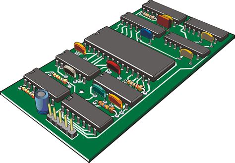
Printed Circuit Board (PCB) sub-assembly is a critical phase in the electronics manufacturing process, involving the integration of various electronic components onto a PCB to create functional modules. This process is essential for ensuring the reliability and performance of electronic devices. To understand the key steps in the PCB sub-assembly process, it is important to delve into the intricacies of each stage, from initial preparation to final inspection.
The process begins with the preparation of the PCB itself.
This involves cleaning the board to remove any contaminants that could interfere with the soldering process. The board is then inspected for any defects or irregularities that could affect its performance. Once the PCB is prepared, the next step is the application of solder paste. Solder paste, a mixture of powdered solder and flux, is applied to the board using a stencil. This ensures that the paste is deposited only on the areas where components will be placed.
Following the application of solder paste, the placement of components is the next crucial step.
This is typically done using automated pick-and-place machines, which accurately position components onto the PCB based on a pre-programmed layout. These machines are capable of placing a wide variety of components, from tiny resistors and capacitors to larger integrated circuits. The precision of this step is vital, as any misalignment can lead to faulty connections and compromised functionality.
Once the components are in place, the assembly moves to the soldering phase.
There are two primary methods of soldering in PCB sub-assembly: reflow soldering and wave soldering. Reflow soldering is commonly used for surface-mount technology (SMT) components. In this method, the PCB is passed through a reflow oven, where the solder paste melts and forms a solid connection between the components and the board. On the other hand, wave soldering is used for through-hole components. In this process, the PCB is passed over a wave of molten solder, which adheres to the exposed metal areas and creates secure connections.
After soldering, the assembled PCB undergoes a thorough cleaning process to remove any residual flux and contaminants.
This is crucial for preventing corrosion and ensuring the long-term reliability of the board. The cleaning process typically involves the use of solvents or specialized cleaning equipment.
The next step in the PCB sub-assembly process is inspection and testing.
This is a multi-faceted stage that includes visual inspection, automated optical inspection (AOI), and functional testing. Visual inspection involves a detailed examination of the board to identify any obvious defects or misalignments. AOI uses advanced imaging technology to detect issues that may not be visible to the naked eye, such as solder joint defects or component misplacements. Functional testing involves powering up the PCB and verifying that it operates as intended. This step is critical for identifying any potential issues before the board is integrated into a larger system.
Finally, once the PCB has passed all inspections and tests, it is ready for packaging and shipment.
Proper packaging is essential to protect the board from damage during transit. This often involves the use of anti-static materials and secure packaging methods to ensure that the PCB arrives at its destination in optimal condition.
In conclusion, the PCB sub-assembly process is a complex and meticulous procedure that requires careful attention to detail at every stage. From initial preparation and component placement to soldering, cleaning, inspection, and packaging, each step plays a vital role in ensuring the quality and reliability of the final product. By adhering to these key steps, manufacturers can produce high-quality PCBs that meet the stringent demands of modern electronic devices.
Common Challenges In PCB Sub Assembly And How To Overcome Them
Printed Circuit Board (PCB) sub-assembly is a critical phase in the electronics manufacturing process, involving the integration of various electronic components onto a PCB. Despite its importance, this stage is fraught with numerous challenges that can impact the overall quality and functionality of the final product. Understanding these common challenges and implementing effective strategies to overcome them is essential for ensuring a successful PCB sub-assembly process.
One of the primary challenges in PCB sub-assembly is component placement accuracy.
The precision with which components are placed on the PCB is crucial, as even minor misalignments can lead to functional defects or complete failure of the electronic device. To address this issue, manufacturers can employ advanced automated placement machines that offer high precision and repeatability. Additionally, implementing rigorous quality control measures, such as optical inspection systems, can help detect and correct placement errors early in the process.
Another significant challenge is soldering quality.
Poor solder joints can result in unreliable electrical connections, leading to intermittent failures or short circuits. To mitigate this risk, it is essential to use high-quality soldering materials and equipment. Moreover, adopting best practices in soldering techniques, such as maintaining optimal temperature profiles and ensuring proper flux application, can significantly enhance solder joint reliability. Regular training and certification of soldering personnel can also contribute to maintaining high standards in soldering quality.
Thermal management is another critical aspect that poses challenges during PCB sub-assembly.
Electronic components generate heat during operation, and inadequate thermal management can lead to overheating, reducing the lifespan and performance of the device. To overcome this challenge, designers can incorporate thermal vias, heat sinks, and thermal pads into the PCB layout. Additionally, using materials with high thermal conductivity and optimizing the placement of heat-generating components can further improve thermal management.
Component compatibility and availability also present challenges in PCB sub-assembly.
The rapid pace of technological advancements often leads to component obsolescence, making it difficult to source compatible parts. To address this issue, manufacturers can establish strong relationships with reliable suppliers and maintain an updated database of alternative components. Furthermore, designing PCBs with flexibility in mind, such as accommodating different package types or footprints, can help mitigate the impact of component shortages.
Electrostatic discharge (ESD) is another concern that can adversely affect PCB sub-assembly.
ESD can damage sensitive electronic components, leading to latent defects that may not be immediately apparent. To prevent ESD-related issues, manufacturers should implement comprehensive ESD control programs, including the use of ESD-safe workstations, tools, and protective clothing. Regular monitoring and auditing of ESD control measures can ensure ongoing compliance and effectiveness.
Finally, maintaining consistent quality and reliability throughout the PCB sub-assembly process is a persistent challenge.
Variability in materials, processes, and human factors can all contribute to inconsistencies. To address this, manufacturers can adopt standardized procedures and protocols, such as those outlined in industry standards like IPC-A-610. Implementing robust process control systems and continuous improvement initiatives, such as Six Sigma or Lean manufacturing, can also help identify and eliminate sources of variability.
In conclusion, while PCB sub-assembly presents several challenges, understanding these issues and implementing effective strategies can significantly enhance the quality and reliability of the final product. By focusing on component placement accuracy, soldering quality, thermal management, component compatibility, ESD control, and process consistency, manufacturers can overcome these challenges and achieve successful PCB sub-assembly outcomes.
Innovations In PCB Sub Assembly Technology
Printed Circuit Board (PCB) sub-assembly technology has undergone significant advancements in recent years, driven by the increasing complexity and miniaturization of electronic devices. These innovations have not only enhanced the performance and reliability of electronic products but have also streamlined the manufacturing process, making it more efficient and cost-effective.
One of the most notable advancements in PCB sub-assembly technology is the development of surface mount technology (SMT).
SMT has revolutionized the way components are mounted onto PCBs, allowing for smaller, lighter, and more compact designs. This technology involves placing components directly onto the surface of the PCB, rather than inserting them through holes. As a result, it has enabled the production of high-density and high-performance electronic assemblies, which are essential for modern applications such as smartphones, laptops, and wearable devices.
In addition to SMT, the advent of advanced materials and fabrication techniques has played a crucial role in the evolution of PCB sub-assembly technology.
For instance, the use of high-frequency laminates and substrates has improved the signal integrity and thermal management of PCBs, making them suitable for high-speed and high-power applications.
Furthermore, the integration of flexible and rigid-flex PCBs has provided designers with greater flexibility in creating complex and space-constrained electronic assemblies. These materials and techniques have not only enhanced the performance of PCBs but have also contributed to the overall miniaturization of electronic devices.
Another significant innovation in PCB sub-assembly technology is the implementation of automated assembly processes.
Automation has greatly improved the precision and consistency of PCB assembly, reducing the likelihood of human error and increasing production yields. Automated optical inspection (AOI) and X-ray inspection systems have become integral parts of the assembly process, ensuring that defects are detected and corrected early in the production cycle. Additionally, the use of robotic pick-and-place machines has accelerated the placement of components, further enhancing the efficiency of the assembly process.
The rise of the Internet of Things (IoT) has also influenced PCB sub-assembly technology, necessitating the development of more sophisticated and interconnected electronic systems.
IoT devices often require PCBs with multiple layers and embedded components to accommodate the various sensors, processors, and communication modules. To meet these demands, manufacturers have adopted advanced techniques such as via-in-pad and microvia technology, which allow for the creation of complex multilayer PCBs with improved electrical performance and reduced size. These innovations have enabled the production of compact and highly functional IoT devices, ranging from smart home appliances to industrial automation systems.
Moreover, the growing emphasis on sustainability and environmental responsibility has led to the adoption of eco-friendly practices in PCB sub-assembly technology.
Manufacturers are increasingly using lead-free soldering processes and environmentally friendly materials to reduce the environmental impact of electronic assemblies. Additionally, advancements in recycling and waste management techniques have facilitated the recovery and reuse of valuable materials from discarded PCBs, contributing to a more sustainable electronics industry.
In conclusion, the continuous advancements in PCB sub-assembly technology have significantly transformed the electronics manufacturing landscape.
From surface mount technology and advanced materials to automated assembly processes and IoT-driven innovations, these developments have enhanced the performance, reliability, and efficiency of electronic products. As the demand for more sophisticated and compact electronic devices continues to grow, it is expected that PCB sub-assembly technology will continue to evolve, driving further innovations and shaping the future of the electronics industry.