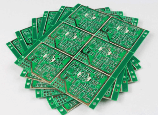
Pcb fab express
Understanding The PCB Fab Express Process: A Step-By-Step Guide
Printed Circuit Board (PCB) fabrication is a critical process in the electronics industry, enabling the creation of complex electronic circuits that power a wide range of devices. The PCB Fab Express process, in particular, is designed to expedite the production of PCBs, ensuring rapid turnaround times without compromising on quality. Understanding this process step-by-step is essential for anyone involved in electronics design and manufacturing.
The first step in the PCB Fab Express process is the design phase.
Engineers and designers use specialized software to create detailed schematics and layouts of the PCB. This digital blueprint includes the placement of components, the routing of electrical connections, and the specification of materials. Once the design is finalized, it is converted into a format compatible with the fabrication equipment, typically Gerber files. These files contain all the necessary information to guide the manufacturing process.
Following the design phase, the next step is the preparation of materials.
High-quality substrates, such as FR4, are selected based on the requirements of the PCB. These substrates serve as the foundation upon which the circuit is built. Copper-clad laminates are then prepared, as copper is the primary conductive material used in PCBs. The copper layer is essential for creating the electrical pathways that connect various components on the board.
Once the materials are ready, the fabrication process begins with the imaging stage.
During this stage, the Gerber files are used to create a photomask, which is a stencil that defines the pattern of the circuit. The photomask is placed over the copper-clad laminate, and ultraviolet (UV) light is used to transfer the circuit pattern onto the laminate. The areas exposed to UV light harden, while the unexposed areas remain soft and are subsequently removed through a chemical etching process. This results in the formation of the copper traces that constitute the circuit.
After imaging, the next step is drilling.
Precision drilling machines create holes in the PCB where components will be mounted. These holes, known as vias, are essential for establishing electrical connections between different layers of the PCB. The accuracy of the drilling process is crucial, as any deviation can affect the performance of the final product.
Following drilling, the PCB undergoes a plating process.
This involves depositing a thin layer of conductive material, typically copper, onto the walls of the drilled holes. This ensures that the vias are electrically conductive, allowing signals to pass between layers. The PCB is then coated with a layer of solder mask, which protects the copper traces from oxidation and prevents short circuits. The solder mask also provides a surface for soldering components onto the board.
The final steps in the PCB Fab Express process include silkscreen printing and testing.
Silkscreen printing involves applying labels and markings to the PCB, which aid in the assembly and identification of components. Once the silkscreen is applied, the PCB undergoes rigorous testing to ensure it meets all design specifications and quality standards. This includes electrical testing to verify the continuity and integrity of the circuits.
In conclusion, the PCB Fab Express process is a streamlined approach to PCB fabrication that emphasizes speed and efficiency. By following a series of well-defined steps, from design and material preparation to imaging, drilling, plating, and testing, manufacturers can produce high-quality PCBs in a short amount of time. Understanding each step of this process is crucial for anyone involved in the electronics industry, as it ensures the successful production of reliable and efficient electronic devices.
Top Benefits Of Using PCB Fab Express For Your Prototyping Needs
When it comes to developing electronic devices, the importance of a reliable and efficient prototyping process cannot be overstated. One of the most critical components in this process is the printed circuit board (PCB), which serves as the backbone of electronic circuits. For engineers and designers, the ability to quickly and accurately produce PCB prototypes is essential. This is where PCB Fab Express comes into play, offering a range of benefits that make it an ideal choice for your prototyping needs.
Firstly, one of the most significant advantages of using PCB Fab Express is the speed of production.
In the fast-paced world of electronics, time is often of the essence. PCB Fab Express specializes in rapid prototyping, allowing you to receive your PCB prototypes in a fraction of the time it would take with traditional manufacturing methods. This accelerated turnaround time enables you to quickly test and iterate on your designs, ultimately speeding up the development cycle and bringing your products to market faster.
In addition to speed, PCB Fab Express also offers a high level of precision and quality.
The company utilizes state-of-the-art manufacturing equipment and adheres to stringent quality control standards. This ensures that each PCB prototype is produced with exceptional accuracy, minimizing the risk of errors and defects. As a result, you can have confidence in the reliability and performance of your prototypes, which is crucial for identifying and addressing potential issues early in the development process.
Moreover, PCB Fab Express provides a wide range of customization options to meet the specific needs of your project.
Whether you require a particular board size, material, or layer count, the company can accommodate your requirements. This flexibility allows you to create prototypes that closely match your final product, providing a more accurate representation of how your design will perform in real-world applications. Additionally, the ability to customize your PCBs can help you explore different design variations and optimize your circuit layout for better performance and efficiency.
Another notable benefit of using PCB Fab Express is the cost-effectiveness of their services.
Prototyping can be an expensive endeavor, especially when dealing with complex and high-precision PCBs. However, PCB Fab Express offers competitive pricing without compromising on quality. By leveraging advanced manufacturing techniques and economies of scale, the company can provide affordable prototyping solutions that fit within your budget. This cost savings can be particularly advantageous for startups and small businesses that need to manage their resources carefully.
Furthermore, PCB Fab Express offers excellent customer support and service.
From the initial design phase to the final delivery of your prototypes, the company’s team of experts is available to assist you at every step. Whether you need help with design optimization, material selection, or troubleshooting, you can rely on their knowledgeable staff to provide valuable guidance and support. This level of customer service ensures a smooth and hassle-free prototyping experience, allowing you to focus on refining your designs and achieving your project goals.
In conclusion, PCB Fab Express stands out as a top choice for your prototyping needs due to its rapid production capabilities, high-quality standards, customization options, cost-effectiveness, and exceptional customer support. By choosing PCB Fab Express, you can streamline your development process, reduce time-to-market, and ensure the reliability and performance of your electronic designs. Whether you are an established company or an emerging startup, leveraging the benefits of PCB Fab Express can significantly enhance your prototyping efforts and contribute to the success of your projects.

How PCB Fab Express Ensures High-Quality Manufacturing Standards
PCB Fab Express is a prominent name in the printed circuit board (PCB) manufacturing industry, known for its commitment to high-quality standards. The company employs a meticulous approach to ensure that every PCB produced meets stringent quality criteria. This dedication to excellence begins with the selection of raw materials. PCB Fab Express sources only the highest-grade materials, ensuring that the foundation of each PCB is robust and reliable. By prioritizing quality from the outset, the company sets the stage for superior end products.
Transitioning from raw materials to the manufacturing process, PCB Fab Express utilizes state-of-the-art technology and equipment.
Advanced machinery and automated systems are integral to their operations, allowing for precision and consistency in production. The use of cutting-edge technology not only enhances efficiency but also minimizes the risk of human error, which is crucial in maintaining high-quality standards. Furthermore, the company continuously invests in upgrading its equipment to stay abreast of technological advancements, ensuring that their manufacturing capabilities remain at the forefront of the industry.
In addition to leveraging advanced technology, PCB Fab Express places a strong emphasis on process control.
Rigorous quality control measures are implemented at every stage of production, from initial design to final inspection. This comprehensive approach ensures that any potential issues are identified and addressed promptly, preventing defects from reaching the customer. The company employs a team of highly skilled engineers and technicians who meticulously monitor each step of the manufacturing process, ensuring adherence to strict quality protocols.
Moreover, PCB Fab Express recognizes the importance of adhering to industry standards and certifications.
The company is ISO 9001 certified, which underscores its commitment to maintaining a quality management system that meets international standards. This certification is a testament to the company’s dedication to continuous improvement and customer satisfaction. Additionally, PCB Fab Express complies with RoHS (Restriction of Hazardous Substances) regulations, ensuring that their products are environmentally friendly and safe for use in various applications.
Customer feedback also plays a pivotal role in PCB Fab Express’s quality assurance strategy.
The company actively seeks input from clients to identify areas for improvement and to ensure that their products meet or exceed customer expectations. By fostering open communication with clients, PCB Fab Express can tailor its services to better meet the specific needs of each customer, further enhancing the quality and reliability of their PCBs.
Furthermore, the company’s commitment to quality extends beyond the manufacturing process to include comprehensive testing and inspection.
PCB undergoes a series of rigorous tests, including electrical testing, thermal cycling, and visual inspection, to verify its performance and durability. These tests are designed to simulate real-world conditions, ensuring that the PCBs can withstand the demands of their intended applications. By subjecting their products to such thorough testing, PCB Fab Express can guarantee the reliability and longevity of their PCBs.
In conclusion, PCB Fab Express’s unwavering commitment to high-quality manufacturing standards is evident in every aspect of their operations. From the careful selection of raw materials to the use of advanced technology and rigorous quality control measures, the company ensures that each PCB produced is of the highest quality. By adhering to industry standards, actively seeking customer feedback, and conducting comprehensive testing, PCB Fab Express consistently delivers reliable and high-performing PCBs that meet the diverse needs of their clients.
Cost-Effective Solutions With PCB Fab Express: Tips And Tricks
Printed Circuit Boards (PCBs) are the backbone of modern electronic devices, and their fabrication is a critical step in the development process. PCB Fab Express has emerged as a popular choice for engineers and designers seeking cost-effective solutions without compromising on quality. To maximize the benefits of using PCB Fab Express, it is essential to understand various tips and tricks that can help in reducing costs while ensuring high-quality outcomes.
One of the primary strategies to achieve cost-effectiveness with PCB Fab Express is to optimize the design for manufacturability.
This involves adhering to standard design rules and guidelines that facilitate efficient production. For instance, maintaining consistent trace widths and spacing, using standard hole sizes, and avoiding complex routing can significantly reduce manufacturing complexity and costs. Additionally, minimizing the number of layers in a PCB design can lead to substantial savings, as multi-layer boards are inherently more expensive to produce.
Another crucial aspect to consider is the selection of materials.
While high-performance materials may be necessary for certain applications, opting for standard materials can often suffice for most projects and result in considerable cost savings. It is also advisable to consult with PCB Fab Express regarding material options, as they can provide valuable insights into cost-effective alternatives that meet the required specifications.
Batch production is another effective way to reduce costs.
By consolidating multiple PCB designs into a single production run, economies of scale can be achieved, leading to lower per-unit costs. PCB Fab Express often offers panelization services, where multiple designs are combined on a single panel, thereby optimizing the use of materials and reducing setup times. This approach is particularly beneficial for small to medium-sized production runs.
Furthermore, taking advantage of the various service options provided by PCB Fab Express can also contribute to cost savings.
For example, opting for standard turnaround times instead of expedited services can significantly lower costs. While expedited services are essential for time-sensitive projects, planning ahead and allowing for standard lead times can result in more economical production.
Effective communication with the PCB Fab Express team is paramount to ensuring a smooth and cost-effective fabrication process.
Providing clear and detailed design files, including Gerber files, Bill of Materials (BOM), and assembly drawings, can help prevent misunderstandings and errors that may lead to costly rework. Additionally, seeking feedback from the fabrication team during the design phase can help identify potential issues early on and allow for timely adjustments.
Another tip for cost-effective PCB fabrication is to leverage the capabilities of PCB design software.
Many modern design tools offer features such as design rule checks (DRC) and electrical rule checks (ERC) that can help identify potential issues before the design is sent for fabrication. Utilizing these tools can help ensure that the design is optimized for manufacturability, thereby reducing the likelihood of costly errors and revisions.
Lastly, staying informed about industry trends and advancements can also contribute to cost savings.
PCB Fab Express, like many other fabrication services, continually updates its processes and technologies to improve efficiency and reduce costs. By staying abreast of these developments, designers and engineers can take advantage of new techniques and materials that offer better performance at lower costs.
In conclusion, achieving cost-effective solutions with PCB Fab Express requires a combination of strategic design practices, material selection, batch production, effective communication, and leveraging design software capabilities. By following these tips and tricks, engineers and designers can optimize their PCB fabrication process, resulting in high-quality boards at a fraction of the cost.