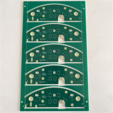
Pcb printing
Innovative Techniques In PCB Printing
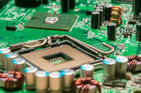
Printed Circuit Board (PCB) printing has undergone significant advancements in recent years, driven by the relentless pursuit of efficiency, precision, and miniaturization in electronic devices. As the backbone of modern electronics, PCBs are integral to the functionality of a wide array of products, from consumer gadgets to industrial machinery. Consequently, innovative techniques in PCB printing have emerged to meet the growing demands for higher performance and reliability.
One of the most notable advancements in PCB printing is the adoption of additive manufacturing techniques.
Unlike traditional subtractive methods, which involve etching away unwanted material from a copper-clad board, additive manufacturing builds the circuit layer by layer. This approach not only reduces material waste but also allows for greater design flexibility. For instance, 3D printing technology has enabled the creation of complex, multi-layered PCBs with intricate geometries that were previously unattainable. This innovation is particularly beneficial for applications requiring compact and lightweight designs, such as wearable technology and aerospace components.
In addition to additive manufacturing, the use of advanced materials has revolutionized PCB printing.
Conductive inks, composed of nanoparticles of metals like silver, copper, and gold, have become increasingly popular. These inks can be precisely deposited onto various substrates using inkjet printing, screen printing, or aerosol jet printing. The result is a highly conductive and reliable circuit that can be produced at a lower cost and with greater speed compared to traditional methods. Moreover, the development of flexible and stretchable substrates has opened new possibilities for PCBs in applications where conventional rigid boards would be impractical, such as in medical devices and flexible displays.
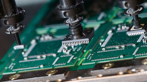
Another significant innovation in PCB printing is the integration of automated optical inspection (AOI) systems.
These systems use high-resolution cameras and sophisticated algorithms to detect defects in the printed circuits at various stages of production. By identifying issues such as misalignments, short circuits, and open circuits early in the manufacturing process, AOI systems help ensure the quality and reliability of the final product. This not only reduces the likelihood of costly recalls and repairs but also enhances the overall efficiency of the production line.
Furthermore, advancements in laser direct imaging (LDI) technology have greatly improved the precision and resolution of PCB printing.
LDI uses laser beams to directly expose the photoresist on the PCB substrate, eliminating the need for photomasks. This method allows for finer line widths and tighter tolerances, which are essential for high-density interconnect (HDI) boards used in advanced electronics. The ability to produce such intricate designs with high accuracy is crucial for meeting the ever-increasing performance requirements of modern electronic devices.
Moreover, the implementation of environmentally friendly practices in PCB printing has gained traction.
Traditional PCB manufacturing processes often involve hazardous chemicals and generate significant waste. However, new techniques such as water-based solder masks and lead-free soldering have been developed to mitigate these environmental impacts. These eco-friendly alternatives not only comply with stringent regulatory standards but also appeal to environmentally conscious consumers and businesses.
In conclusion, the field of PCB printing is experiencing a transformative phase, driven by innovative techniques that enhance efficiency, precision, and sustainability. Additive manufacturing, advanced materials, automated inspection systems, laser direct imaging, and environmentally friendly practices are at the forefront of this evolution. As technology continues to advance, these innovations will undoubtedly play a crucial role in shaping the future of electronics, enabling the development of more sophisticated, reliable, and eco-friendly devices.
The Future Of PCB Printing Technology
The future of PCB printing technology is poised to revolutionize the electronics industry, driven by advancements in materials science, manufacturing processes, and design methodologies. As the demand for smaller, more efficient, and highly integrated electronic devices continues to grow, the need for innovative PCB printing solutions becomes increasingly critical. One of the most significant developments in this field is the advent of additive manufacturing techniques, which offer unprecedented flexibility and precision in PCB fabrication.
Additive manufacturing, commonly known as 3D printing, has made significant strides in recent years, enabling the production of complex, multi-layered PCBs with intricate geometries that were previously unattainable using traditional subtractive methods.
This technology allows for the direct printing of conductive materials, insulating layers, and even components onto a substrate, thereby reducing the number of manufacturing steps and minimizing material waste. Consequently, additive manufacturing not only enhances the efficiency of PCB production but also opens up new possibilities for custom and on-demand manufacturing.
In addition to additive manufacturing, advancements in materials science are playing a crucial role in shaping the future of PCB printing technology.
The development of novel conductive inks and substrates has expanded the range of materials that can be used in PCB fabrication, offering improved electrical performance, thermal management, and mechanical properties. For instance, the incorporation of nanomaterials such as graphene and carbon nanotubes into conductive inks has shown promise in enhancing the conductivity and flexibility of printed circuits. Moreover, the use of flexible substrates like polyimide and polyethylene terephthalate (PET) enables the creation of flexible and wearable electronics, which are becoming increasingly popular in applications ranging from healthcare to consumer electronics.
Another key factor driving the evolution of PCB printing technology is the integration of advanced design software and simulation tools.
These tools facilitate the design and optimization of complex PCB layouts, allowing engineers to predict and mitigate potential issues such as signal integrity, thermal management, and electromagnetic interference. By leveraging these sophisticated design tools, manufacturers can achieve higher levels of precision and reliability in their PCB designs, ultimately leading to better-performing electronic devices.
Furthermore, the rise of the Internet of Things (IoT) and the proliferation of connected devices are fueling the demand for innovative PCB solutions.
IoT devices often require compact, low-power, and highly integrated PCBs to accommodate their small form factors and energy-efficient operation. In response to this demand, PCB printing technology is evolving to support the production of miniaturized and highly integrated circuits, enabling the development of next-generation IoT devices that are more powerful and versatile than ever before.
In conclusion, the future of PCB printing technology is being shaped by a confluence of advancements in additive manufacturing, materials science, and design methodologies. These innovations are driving the development of more efficient, flexible, and high-performance PCBs, which are essential for meeting the growing demands of the electronics industry. As these technologies continue to mature, we can expect to see even more groundbreaking developments in PCB printing, ultimately leading to the creation of electronic devices that are smaller, faster, and more capable than ever before. The ongoing evolution of PCB printing technology promises to unlock new possibilities and applications, heralding a new era of innovation in the world of electronics.
Common Challenges In PCB Printing And How To Overcome Them
Printed Circuit Board (PCB) printing is a critical process in the manufacturing of electronic devices, serving as the backbone for electrical connectivity and component support. Despite its importance, PCB printing is fraught with numerous challenges that can impact the quality, functionality, and reliability of the final product. Understanding these common challenges and knowing how to overcome them is essential for ensuring successful PCB production.
One of the primary challenges in PCB printing is achieving precise alignment and registration.
Misalignment can lead to short circuits, open circuits, and other functional defects. This issue often arises due to inaccuracies in the photolithography process, where the photoresist layer is exposed to UV light through a mask. To mitigate this problem, manufacturers can employ advanced alignment systems that use optical recognition to ensure precise positioning. Additionally, regular calibration of equipment and thorough inspection of masks can help maintain alignment accuracy.
Another significant challenge is managing the thermal properties of the PCB.
During the soldering process, components are subjected to high temperatures, which can cause warping or delamination of the board. This thermal stress can compromise the structural integrity and performance of the PCB. To address this, manufacturers can use materials with high thermal stability and employ controlled cooling techniques to minimize thermal shock. Furthermore, designing the PCB with appropriate thermal reliefs and vias can help dissipate heat more effectively.
Contamination is also a prevalent issue in PCB printing.
Dust, oils, and other contaminants can interfere with the adhesion of photoresist and solder mask layers, leading to defects such as poor etching and solder bridging. To combat contamination, maintaining a cleanroom environment is crucial. Implementing stringent cleaning protocols for both the PCB and the manufacturing equipment can significantly reduce the risk of contamination. Additionally, using high-purity chemicals and materials can further enhance the cleanliness of the process.
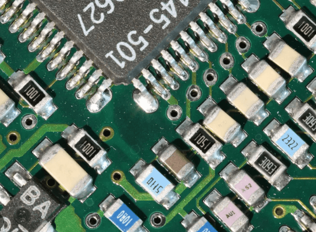
The complexity of modern PCBs, with their high component density and fine pitch, presents another challenge.
As the demand for smaller and more powerful electronic devices grows, the need for miniaturized components and intricate designs increases. This complexity can lead to difficulties in achieving accurate etching and soldering. To overcome this, manufacturers can utilize advanced fabrication techniques such as laser direct imaging (LDI) and precision etching processes. These technologies offer higher resolution and accuracy, enabling the production of complex PCB designs with minimal defects.
Electrical performance is another critical aspect that can be affected by various factors during PCB printing.
Impedance control, signal integrity, and electromagnetic interference (EMI) are all concerns that must be addressed to ensure optimal performance. To manage these issues, careful design considerations are necessary. This includes selecting appropriate materials, optimizing trace widths and spacing, and incorporating shielding and grounding techniques. Simulation tools can also be employed to predict and mitigate potential electrical performance issues before the manufacturing stage.
In conclusion, PCB printing is a complex process that involves numerous challenges, from alignment and thermal management to contamination and electrical performance. By understanding these challenges and implementing appropriate solutions, manufacturers can enhance the quality and reliability of their PCBs. Advanced technologies, stringent cleanliness protocols, and meticulous design considerations are all essential components in overcoming the obstacles associated with PCB printing. Through continuous improvement and innovation, the industry can continue to meet the evolving demands of modern electronics.
Environmental Impact Of PCB Printing And Sustainable Practices
The environmental impact of PCB printing is a multifaceted issue that encompasses various stages of the manufacturing process, from raw material extraction to waste disposal. Printed Circuit Boards (PCBs) are indispensable in modern electronics, yet their production poses significant environmental challenges. The primary materials used in PCB manufacturing include copper, fiberglass, and various chemicals, all of which have environmental footprints. Copper mining, for instance, is energy-intensive and often results in habitat destruction and water pollution. Similarly, the production of fiberglass involves the use of non-renewable resources and emits greenhouse gases.
Transitioning to the manufacturing process itself, the etching and plating stages are particularly concerning.
These processes involve the use of hazardous chemicals such as ferric chloride and ammonium persulfate, which can contaminate water sources if not properly managed. Additionally, the energy consumption in PCB manufacturing is substantial, contributing to carbon emissions. The disposal of chemical waste is another critical issue, as improper handling can lead to soil and water contamination, posing risks to both human health and ecosystems.
In light of these environmental concerns, sustainable practices in PCB printing are gaining traction.
One of the most effective strategies is the adoption of green chemistry principles, which aim to reduce or eliminate the use of hazardous substances. For example, some manufacturers are exploring the use of less toxic etching solutions and developing methods to recycle etching chemicals. Furthermore, advancements in additive manufacturing, such as inkjet printing of conductive inks, offer promising alternatives to traditional subtractive methods, thereby reducing material waste.
Energy efficiency is another area where sustainable practices can make a significant impact.
Implementing energy-efficient machinery and optimizing production processes can substantially reduce the carbon footprint of PCB manufacturing. Renewable energy sources, such as solar or wind power, can also be integrated into the production process to further mitigate environmental impact. Additionally, some companies are investing in carbon offset programs to balance their emissions, although this should be seen as a supplementary measure rather than a primary solution.
Waste management is equally crucial in promoting sustainability in PCB printing.
Recycling and reusing materials can significantly reduce the environmental burden. For instance, copper can be recovered from waste PCBs and reused in new boards, thereby conserving natural resources and reducing the need for mining. Similarly, initiatives to recycle fiberglass and other non-metallic components are being developed, although these are still in the nascent stages.
Moreover, the concept of a circular economy is gaining relevance in the context of PCB manufacturing.
This approach emphasizes the importance of designing products for longevity, repairability, and recyclability. By extending the lifecycle of PCBs and facilitating their reuse, the demand for new raw materials can be minimized, thereby reducing environmental impact. Companies are also encouraged to adopt take-back programs, where end-of-life PCBs are returned to the manufacturer for recycling or safe disposal.
In conclusion, while the environmental impact of PCB printing is significant, there are numerous sustainable practices that can mitigate these effects. From adopting green chemistry and energy-efficient technologies to implementing robust waste management and recycling programs, the industry has multiple avenues to pursue sustainability. As consumer awareness and regulatory pressures continue to grow, it is imperative for PCB manufacturers to integrate these practices into their operations, thereby contributing to a more sustainable future.
Step-By-Step Guide To DIY PCB Printing
Printed Circuit Boards (PCBs) are the backbone of modern electronic devices, providing the necessary pathways for electrical currents to flow between components. While commercial PCB manufacturing is a highly specialized process, DIY PCB printing has become increasingly accessible, allowing hobbyists and small-scale developers to create custom boards at home. This step-by-step guide aims to elucidate the process of DIY PCB printing, ensuring that even those new to the field can achieve satisfactory results.
To begin with, the initial step in DIY PCB printing involves designing the circuit layout.
This is typically done using specialized software such as Eagle, KiCad, or Altium Designer. These programs allow users to create a schematic diagram of the circuit, which is then converted into a PCB layout. It is crucial to ensure that the design adheres to the necessary electrical standards and that the components are correctly placed to avoid any potential issues during the manufacturing process.
Once the design is finalized, the next step is to print the PCB layout onto a transparent film.
This is usually done using a laser printer, as inkjet printers may not provide the required precision. The transparency film serves as a mask for the subsequent photoresist process. It is important to ensure that the printed layout is accurate and free of any smudges or defects, as these can affect the quality of the final PCB.
Following the printing of the layout, the next phase involves preparing the copper-clad board.
This board is coated with a layer of photoresist, a light-sensitive material that hardens when exposed to ultraviolet (UV) light. The transparency film is then placed over the photoresist-coated board, and the assembly is exposed to UV light. The areas of the photoresist that are exposed to the light harden, while the unexposed areas remain soft and can be washed away using a developer solution.
After developing the board, the next step is etching.
This process involves submerging the board in an etching solution, typically ferric chloride or ammonium persulfate, which dissolves the unprotected copper, leaving behind only the desired circuit pattern. It is essential to handle the etching solution with care, as it is highly corrosive and can cause damage if not used properly. The etching process should be monitored closely to ensure that all unwanted copper is removed without over-etching the desired circuit paths.
Once the etching is complete, the board is thoroughly cleaned to remove any remaining photoresist and etching solution.
This can be done using acetone or a similar solvent. The next step involves drilling holes for the component leads. This requires a precision drill, as the holes must be accurately placed to match the component layout. Care must be taken to avoid damaging the circuit paths during this process.
The final step in DIY PCB printing is soldering the components onto the board. This involves placing the components in their respective positions and using a soldering iron to attach them to the copper pads. It is important to ensure that the solder joints are clean and free of any excess solder, as poor soldering can lead to unreliable connections and potential circuit failures.
In conclusion, DIY PCB printing is a meticulous process that requires careful attention to detail at each step. From designing the circuit layout to soldering the final components, each phase plays a crucial role in ensuring the quality and functionality of the finished PCB. By following this step-by-step guide, hobbyists and small-scale developers can successfully create custom PCBs, enabling them to bring their electronic projects to life.