Pcb manufacturing requirements
Essential Design Guidelines For PCB Manufacturing
Printed Circuit Board (PCB) manufacturing is a complex process that requires meticulous attention to detail and adherence to specific design guidelines to ensure functionality, reliability, and manufacturability.
One of the primary considerations in PCB design is the selection of materials.
The substrate material, typically FR-4, must be chosen based on the application’s thermal, electrical, and mechanical requirements. Additionally, the copper thickness, which affects current-carrying capacity and thermal management, must be specified accurately.
Transitioning to the layout design, trace width and spacing are critical parameters.
The trace width must be sufficient to handle the expected current without excessive heating, while the spacing between traces must prevent electrical shorts and crosstalk. Design rules for trace width and spacing are often dictated by industry standards such as IPC-2221, which provides guidelines based on the current-carrying capacity and voltage levels.
Another essential aspect is the placement of components.
Proper component placement not only affects the electrical performance but also the manufacturability and ease of assembly. Components should be placed to minimize the length of critical signal paths and to ensure that heat-generating components are adequately spaced to prevent thermal issues. Furthermore, the orientation of components should be consistent to facilitate automated assembly processes.
Via design is another crucial element in PCB manufacturing.
Vias, which are used to connect different layers of a PCB, must be designed with appropriate diameters and annular rings to ensure reliable electrical connections. The aspect ratio of vias, which is the ratio of the board thickness to the via diameter, should be kept within manufacturable limits to avoid issues during the plating process.
Moving on to signal integrity, controlled impedance is vital for high-speed digital circuits.
Impedance control is achieved by carefully designing the trace width, spacing, and the distance from the reference plane. Differential pairs, which are used for high-speed signals, must be routed with consistent spacing and length matching to ensure signal integrity.
Thermal management is another critical consideration in PCB design.
Heat sinks, thermal vias, and copper pours are commonly used to dissipate heat from high-power components. The thermal design must ensure that the PCB can operate within the specified temperature range without compromising performance or reliability.
Design for manufacturability (DFM) principles must also be integrated into the PCB design process.
DFM involves designing the PCB in a way that simplifies the manufacturing process, reduces costs, and minimizes the risk of defects. This includes considerations such as panelization, which optimizes the use of PCB material and facilitates efficient assembly, and the use of standard component footprints to ensure compatibility with automated assembly equipment.
In addition to these technical considerations, documentation is a vital part of the PCB design process.
Comprehensive documentation, including schematics, layout files, and a bill of materials (BOM), is essential for successful manufacturing. Clear and detailed documentation helps manufacturers understand the design intent and ensures that the PCB is built to the correct specifications.
In conclusion, PCB manufacturing requires a thorough understanding of material properties, layout design, signal integrity, thermal management, and manufacturability principles. By adhering to these essential design guidelines, designers can create PCBs that meet performance requirements, are reliable, and can be manufactured efficiently. The integration of these guidelines into the design process is crucial for the successful production of high-quality PCBs.
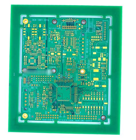
Material Selection Criteria In PCB Production
In the realm of printed circuit board (PCB) manufacturing, the selection of materials is a critical factor that significantly influences the performance, reliability, and longevity of the final product. The choice of materials must be meticulously considered to meet the specific requirements of the application, as well as to comply with industry standards and regulations.
To begin with, the substrate material forms the foundation of the PCB and is typically made from fiberglass-reinforced epoxy resin, known as FR-4.
This material is favored for its excellent mechanical strength, thermal stability, and electrical insulation properties. However, for high-frequency applications, materials such as polytetrafluoroethylene (PTFE) or ceramic-filled substrates may be preferred due to their superior dielectric properties and lower signal loss.
Transitioning to the conductive layers, copper is the material of choice for creating the intricate circuitry on PCBs.
Copper’s high electrical conductivity ensures efficient signal transmission and minimal power loss. The thickness of the copper layer, often measured in ounces per square foot, is selected based on the current-carrying requirements of the circuit. For instance, thicker copper layers are used in power electronics to handle higher currents, while thinner layers suffice for signal processing applications. Additionally, the copper surface is typically treated with a protective coating, such as immersion gold or organic solderability preservative (OSP), to prevent oxidation and ensure reliable soldering.
Moving on to the solder mask, this layer is applied over the copper traces to insulate and protect them from environmental factors and to prevent short circuits.
The solder mask material is usually a liquid photoimageable (LPI) epoxy that is cured using ultraviolet (UV) light. The color of the solder mask, often green, is chosen for its contrast with the copper traces, aiding in visual inspection and troubleshooting. However, other colors like red, blue, and black are also available based on aesthetic preferences or specific application needs.
Furthermore, the silkscreen layer, which is used to print component labels, logos, and other markings on the PCB, is typically made from non-conductive epoxy ink.
This layer aids in the assembly process by providing clear identification of component placement and orientation. The choice of silkscreen material must ensure good adhesion to the solder mask and resistance to the soldering process’s heat.
In addition to these primary materials, the selection of adhesives and laminates is crucial for multi-layer PCBs.
These materials must exhibit excellent bonding properties, thermal stability, and minimal dielectric loss to maintain the integrity and performance of the PCB stack-up. Advanced laminates, such as polyimide or high-temperature FR-4, are often used in applications requiring high thermal endurance, such as aerospace and automotive electronics.
Moreover, environmental and regulatory considerations play a significant role in material selection.
Compliance with standards such as RoHS (Restriction of Hazardous Substances) and REACH (Registration, Evaluation, Authorization, and Restriction of Chemicals) is mandatory to ensure that the materials used do not contain harmful substances and are safe for both the environment and human health.
In conclusion, the material selection criteria in PCB production encompass a comprehensive evaluation of mechanical, electrical, thermal, and environmental properties. Each material choice, from the substrate to the conductive layers, solder mask, silkscreen, adhesives, and laminates, must be carefully aligned with the specific requirements of the application and industry standards. This meticulous selection process ensures the production of high-quality, reliable, and durable PCBs that meet the ever-evolving demands of modern electronic devices.
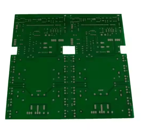
Quality Control Measures In PCB Fabrication
In the realm of printed circuit board (PCB) fabrication, quality control measures are paramount to ensuring the reliability and performance of the final product. The intricate nature of PCBs, which serve as the backbone of virtually all electronic devices, necessitates rigorous quality control protocols throughout the manufacturing process. These measures are designed to detect and mitigate potential defects, ensuring that each PCB meets stringent industry standards and customer specifications.
To begin with, the initial stage of PCB fabrication involves the careful selection of raw materials.
High-quality substrates, copper foils, and laminates are essential to the integrity of the final product. Suppliers are meticulously vetted, and materials are subjected to thorough inspections upon arrival. This preliminary step is crucial, as any compromise in material quality can lead to significant issues down the line.
Following material selection, the design and layout of the PCB are scrutinized through a process known as Design for Manufacturability (DFM) analysis.
This step ensures that the design can be efficiently and accurately produced, minimizing the risk of errors during fabrication. DFM analysis involves checking for potential issues such as insufficient spacing between components, incorrect pad sizes, and other design flaws that could impact the manufacturing process.
As the PCB moves into the production phase, several critical quality control measures come into play.
One of the most important is the use of automated optical inspection (AOI) systems. These systems employ high-resolution cameras and advanced algorithms to inspect the PCB for defects such as misaligned components, solder bridges, and other anomalies. AOI systems are capable of detecting even the smallest imperfections, ensuring that each PCB meets the required specifications.
In addition to AOI, X-ray inspection is employed to examine the internal structure of the PCB.
This non-destructive testing method is particularly useful for detecting hidden defects such as voids in solder joints, misaligned layers, and other internal issues that are not visible to the naked eye. By providing a detailed view of the PCB’s internal composition, X-ray inspection helps to ensure the structural integrity and reliability of the final product.
Electrical testing is another critical component of the quality control process.
This involves subjecting the PCB to a series of tests to verify its electrical performance. Continuity tests check for open circuits, while isolation tests ensure that there are no unintended connections between different parts of the circuit. Additionally, functional testing may be conducted to simulate the PCB’s operation in its intended application, further verifying its performance and reliability.
Throughout the manufacturing process, strict adherence to industry standards and certifications is maintained.
Standards such as IPC-A-600 and IPC-6012 provide guidelines for the acceptability of PCBs, covering aspects such as material quality, workmanship, and performance. Compliance with these standards is essential to ensuring that the final product meets the highest levels of quality and reliability.
Finally, documentation and traceability are integral to the quality control process.
Detailed records of each step in the manufacturing process, including material lot numbers, inspection results, and test data, are meticulously maintained. This documentation not only facilitates traceability in the event of a defect but also provides valuable data for continuous improvement efforts.
In conclusion, quality control measures in PCB fabrication are comprehensive and multifaceted, encompassing everything from material selection and design analysis to advanced inspection techniques and rigorous testing. By implementing these measures, manufacturers can ensure that each PCB meets the highest standards of quality and reliability, ultimately contributing to the success and longevity of the electronic devices they support.
Environmental Considerations In PCB Manufacturing
Printed Circuit Board (PCB) manufacturing is a complex process that involves various stages, each with its own set of environmental considerations. As the demand for electronic devices continues to grow, so does the need for sustainable practices in PCB production.
One of the primary environmental concerns in PCB manufacturing is the use of hazardous chemicals.
These chemicals, such as etchants, solvents, and plating solutions, are essential for creating the intricate patterns on the boards. However, improper handling and disposal of these substances can lead to soil and water contamination. To mitigate this risk, manufacturers must adhere to strict regulations and implement effective waste management systems.
In addition to chemical usage, energy consumption is another critical factor.
The PCB manufacturing process is energy-intensive, involving multiple stages such as drilling, plating, and soldering. Each of these stages requires significant amounts of electricity, contributing to the overall carbon footprint of the production process. To address this issue, manufacturers are increasingly adopting energy-efficient technologies and practices. For instance, the use of LED lighting, energy-efficient machinery, and renewable energy sources can significantly reduce energy consumption and greenhouse gas emissions.
Water usage is also a significant environmental consideration in PCB manufacturing.
The process requires large volumes of water for rinsing and cleaning the boards at various stages. This not only leads to high water consumption but also generates substantial amounts of wastewater. The wastewater often contains harmful chemicals and heavy metals, posing a threat to aquatic ecosystems if not treated properly. Therefore, implementing advanced water treatment systems and recycling processes is crucial for minimizing the environmental impact.
Moreover, the choice of materials plays a vital role in the sustainability of PCB manufacturing.
Traditional PCBs are made from materials such as fiberglass and epoxy resins, which are not biodegradable and can persist in the environment for long periods. To address this issue, researchers and manufacturers are exploring alternative materials that are more environmentally friendly. For example, the use of biodegradable substrates and lead-free solder can significantly reduce the environmental footprint of PCBs.
Another important aspect is the end-of-life management of PCBs.
Electronic waste, or e-waste, is a growing concern globally, with millions of tons generated each year. PCBs are a significant component of e-waste, and improper disposal can lead to the release of toxic substances into the environment. To combat this, manufacturers are increasingly focusing on designing PCBs that are easier to recycle. This includes using materials that can be easily separated and recovered, as well as designing for disassembly.
Furthermore, regulatory compliance is essential for ensuring that PCB manufacturing processes are environmentally responsible.
Various international and national regulations govern the use of hazardous substances, waste management, and emissions in PCB production. Compliance with these regulations not only helps in reducing environmental impact but also ensures that manufacturers can operate in global markets without facing legal and financial penalties.
In conclusion, environmental considerations in PCB manufacturing encompass a wide range of factors, from chemical usage and energy consumption to water usage and material selection. By adopting sustainable practices and technologies, manufacturers can significantly reduce the environmental impact of PCB production. This not only helps in preserving natural resources and protecting ecosystems but also aligns with the growing consumer demand for environmentally responsible products. As the industry continues to evolve, ongoing research and innovation will be crucial in developing more sustainable solutions for PCB manufacturing.
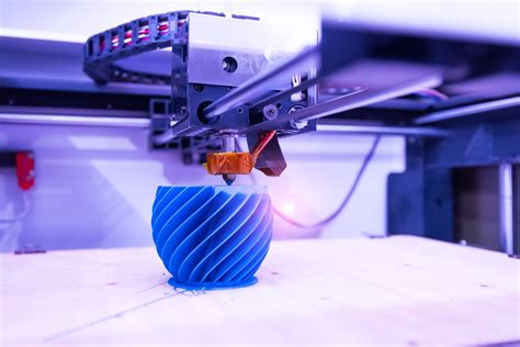
Advanced Techniques In PCB Prototyping
In the realm of printed circuit board (PCB) manufacturing, the advent of advanced techniques in PCB prototyping has significantly transformed the landscape, enabling more efficient, precise, and innovative designs. As the demand for more complex and high-performance electronic devices continues to grow, the need for sophisticated prototyping methods becomes increasingly critical. These advanced techniques not only streamline the development process but also enhance the overall quality and functionality of the final product.
One of the foremost advancements in PCB prototyping is the utilization of computer-aided design (CAD) software.
CAD tools have revolutionized the way engineers and designers approach PCB layout and design. By leveraging these sophisticated software solutions, designers can create highly detailed and accurate representations of their circuits, allowing for meticulous planning and optimization. This digital approach facilitates the identification and rectification of potential issues early in the design phase, thereby reducing the likelihood of costly errors during manufacturing.
Transitioning from design to physical prototyping, additive manufacturing, commonly known as 3D printing, has emerged as a game-changer in PCB prototyping.
This technique allows for the rapid creation of complex PCB structures with high precision. Unlike traditional subtractive methods, which involve etching away material to form the desired circuit patterns, additive manufacturing builds the PCB layer by layer. This not only minimizes material waste but also enables the production of intricate designs that would be challenging or impossible to achieve with conventional methods. Furthermore, 3D printing can significantly shorten the prototyping cycle, allowing for faster iteration and refinement of designs.
Another critical advancement in PCB prototyping is the implementation of advanced materials.
Traditional PCBs are typically made from materials such as FR4, a composite of woven fiberglass cloth with an epoxy resin binder. However, the increasing demand for high-frequency and high-speed applications has necessitated the use of advanced materials like Rogers laminates and polyimide substrates. These materials offer superior electrical properties, such as lower dielectric constant and dissipation factor, which are essential for maintaining signal integrity in high-performance circuits. Additionally, advanced materials often exhibit better thermal stability and mechanical strength, enhancing the durability and reliability of the final product.
In conjunction with advanced materials, the adoption of high-density interconnect (HDI) technology has become a pivotal aspect of modern PCB prototyping.
HDI technology involves the use of microvias, blind vias, and buried vias to create more compact and densely packed circuit boards. This technique is particularly beneficial for applications where space is at a premium, such as in mobile devices and wearable technology. By enabling more connections in a smaller area, HDI technology allows for greater functionality and performance without increasing the overall size of the PCB.
Moreover, the integration of automated testing and inspection systems has further refined the PCB prototyping process.
Automated optical inspection (AOI) and automated X-ray inspection (AXI) systems are now commonly employed to ensure the accuracy and quality of PCB prototypes. These systems can quickly and accurately detect defects such as misaligned components, soldering issues, and trace discontinuities, thereby ensuring that only high-quality prototypes proceed to the next stage of development.
In conclusion, the advancements in PCB prototyping techniques have ushered in a new era of innovation and efficiency in electronic design and manufacturing. From the use of CAD software and 3D printing to the implementation of advanced materials and HDI technology, these techniques collectively enhance the precision, functionality, and reliability of PCB prototypes. As technology continues to evolve, it is imperative for designers and manufacturers to stay abreast of these advancements to maintain a competitive edge in the ever-changing landscape of electronics.