Mfs flex pcb
Advantages Of Using MFS Flex PCB In Modern Electronics
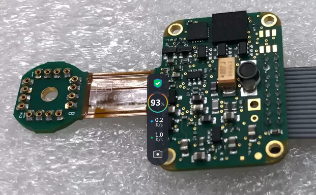
The integration of MFS (Multi-Functional Substrate) Flex PCBs in modern electronics has revolutionized the industry, offering a myriad of advantages that enhance both the performance and reliability of electronic devices.
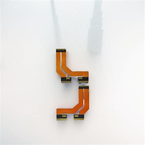
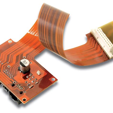
One of the primary benefits of MFS Flex PCBs is their remarkable flexibility, which allows for the design of more compact and lightweight devices.
This flexibility is particularly advantageous in applications where space is at a premium, such as in wearable technology, medical devices, and advanced consumer electronics. By enabling the creation of intricate and compact designs, MFS Flex PCBs contribute to the miniaturization trend that is prevalent in today’s electronics market.
In addition to their flexibility, MFS Flex PCBs are known for their excellent thermal management properties.
The materials used in these substrates are designed to dissipate heat efficiently, which is crucial for maintaining the performance and longevity of electronic components. Effective thermal management reduces the risk of overheating, thereby enhancing the reliability and durability of the device. This is especially important in high-performance applications, such as in automotive electronics and industrial machinery, where maintaining optimal operating temperatures is critical.
Moreover, MFS Flex PCBs offer superior electrical performance compared to traditional rigid PCBs.
The use of advanced materials and manufacturing techniques results in lower signal loss and higher signal integrity. This is particularly beneficial in high-frequency applications, where maintaining signal quality is essential. The improved electrical performance of MFS Flex PCBs ensures that devices can operate at higher speeds and with greater efficiency, meeting the ever-increasing demands for faster and more reliable electronic systems.
Another significant advantage of MFS Flex PCBs is their ability to withstand harsh environmental conditions.
These substrates are designed to be highly resistant to moisture, chemicals, and mechanical stress, making them ideal for use in rugged environments. This durability ensures that electronic devices can function reliably in a wide range of conditions, from extreme temperatures to high humidity levels. As a result, MFS Flex PCBs are widely used in aerospace, military, and outdoor applications, where reliability and robustness are paramount.
Furthermore, the use of MFS Flex PCBs can lead to cost savings in the manufacturing process.
The ability to integrate multiple functions into a single substrate reduces the need for additional components and interconnections, simplifying the assembly process. This not only lowers material costs but also reduces labor and production time. Additionally, the enhanced reliability and durability of MFS Flex PCBs can lead to lower maintenance and repair costs over the lifespan of the device, providing further economic benefits.
In conclusion, the advantages of using MFS Flex PCBs in modern electronics are manifold. Their flexibility, superior thermal management, excellent electrical performance, and durability make them an ideal choice for a wide range of applications. Moreover, the potential for cost savings in manufacturing and maintenance further underscores their value in the electronics industry. As technology continues to advance, the adoption of MFS Flex PCBs is likely to increase, driving innovation and enabling the development of more sophisticated and reliable electronic devices.
Design Considerations For MFS Flex PCB Applications
When designing MFS (Multi-Functional Substrate) flex PCBs, several critical considerations must be taken into account to ensure optimal performance and reliability. The unique properties of flexible printed circuit boards, combined with the multifunctional capabilities of MFS technology, necessitate a thorough understanding of both material selection and design intricacies.
To begin with, material selection is paramount in the design of MFS flex PCBs.
The choice of substrate material directly impacts the flexibility, durability, and thermal management of the final product. Polyimide is a commonly used material due to its excellent thermal stability and mechanical properties. However, depending on the specific application requirements, other materials such as polyester or liquid crystal polymer may be considered. These materials offer varying degrees of flexibility and thermal performance, which must be matched to the operational environment of the PCB.
In addition to material selection, the layout and routing of the circuit traces are crucial.
The flexibility of the PCB allows for more complex and compact designs, but it also introduces challenges in maintaining signal integrity and minimizing electromagnetic interference (EMI). Careful planning of trace width, spacing, and routing paths is essential to mitigate these issues. Utilizing ground planes and shielding techniques can further enhance signal integrity and reduce EMI, ensuring reliable operation in high-frequency applications.
Thermal management is another critical aspect of MFS flex PCB design.
The compact nature of these circuits often leads to higher power densities, which can result in significant heat generation. Effective thermal management strategies, such as the incorporation of thermal vias, heat sinks, and the use of thermally conductive materials, are necessary to dissipate heat and maintain the performance and longevity of the PCB. Additionally, thermal simulations during the design phase can help identify potential hotspots and optimize the thermal performance of the final product.
Mechanical considerations also play a significant role in the design of MFS flex PCBs
The flexible nature of these circuits allows them to be bent, folded, and twisted, which can introduce mechanical stress and potential failure points. Designing for mechanical reliability involves selecting appropriate bend radii, reinforcing critical areas with stiffeners, and ensuring that the flexing does not exceed the material’s mechanical limits. Furthermore, understanding the operational environment, including factors such as vibration and mechanical shock, is essential to ensure the PCB can withstand the intended use conditions.
Moreover, the integration of multiple functions within a single substrate requires careful consideration of component placement and interconnectivity.
The compact design of MFS flex PCBs often necessitates the use of fine-pitch components and high-density interconnects, which can complicate the assembly process. Advanced manufacturing techniques, such as laser drilling and precision placement equipment, are often required to achieve the necessary accuracy and reliability. Additionally, thorough testing and validation are essential to ensure that all integrated functions operate correctly and do not interfere with each other.
In conclusion, the design of MFS flex PCBs involves a complex interplay of material selection, electrical and thermal management, mechanical reliability, and advanced manufacturing techniques. By carefully considering these factors and employing best practices throughout the design and manufacturing process, it is possible to create highly reliable and efficient MFS flex PCBs that meet the demanding requirements of modern electronic applications.
Manufacturing Process Of MFS Flex PCB: A Step-By-Step Guide
The manufacturing process of MFS (Multi-Flex System) Flex PCBs is a sophisticated and intricate procedure that demands precision and expertise. This process begins with the selection of appropriate materials, which is crucial for ensuring the flexibility and durability of the final product. Typically, polyimide films are chosen due to their excellent thermal stability and mechanical properties. These films serve as the substrate upon which the circuit is built.
Once the substrate is selected, the next step involves the application of a conductive layer, usually copper, onto the polyimide film.
This is achieved through a process known as lamination, where the copper foil is bonded to the substrate under heat and pressure. Following this, the laminated material undergoes a cleaning process to remove any contaminants that could affect the subsequent steps.
The cleaned laminate is then subjected to a photolithography process, which is essential for defining the circuit pattern. During this stage, a photoresist material is applied to the copper surface. The photoresist is then exposed to ultraviolet light through a photomask that contains the desired circuit pattern. The areas of the photoresist exposed to the light harden, while the unexposed areas remain soft and can be washed away, revealing the underlying copper.
Subsequently, the exposed copper is etched away using a chemical solution, leaving behind the circuit pattern defined by the hardened photoresist.
After etching, the remaining photoresist is stripped away, revealing the copper circuit on the polyimide substrate. This step is critical as it ensures the accuracy and integrity of the circuit design.
Following the etching process, the next phase involves drilling holes, known as vias, into the PCB. These vias are essential for creating electrical connections between different layers of the PCB. The drilling can be performed using mechanical drills or laser technology, depending on the precision required. Once the vias are drilled, they are plated with copper to establish the necessary electrical connections.
The PCB then undergoes a series of inspections and tests to ensure that it meets the required specifications.
These inspections include visual checks, electrical testing, and sometimes even X-ray analysis to verify the integrity of the vias and the overall circuit. Any defects identified during these inspections are addressed before proceeding to the next stage.
After passing the inspections, the PCB is coated with a protective layer, often referred to as a solder mask. This layer protects the copper circuits from oxidation and prevents solder bridges during the assembly process. The solder mask is applied using a screen-printing technique and then cured under ultraviolet light.
The final step in the manufacturing process is the application of surface finishes, which enhance the solderability of the PCB.
Common finishes include HASL (Hot Air Solder Leveling), ENIG (Electroless Nickel Immersion Gold), and OSP (Organic Solderability Preservative). Each finish has its advantages and is selected based on the specific requirements of the application.
In conclusion, the manufacturing process of MFS Flex PCBs is a meticulous and multi-step procedure that involves material selection, lamination, photolithography, etching, drilling, inspection, and finishing. Each step is critical in ensuring the quality and performance of the final product. By adhering to these precise manufacturing processes, manufacturers can produce high-quality MFS Flex PCBs that meet the demanding requirements of modern electronic applications.
Common Challenges And Solutions In MFS Flex PCB Implementation
The implementation of MFS (Multi-Functional Substrate) flex PCBs (Printed Circuit Boards) has become increasingly prevalent in various industries due to their versatility and efficiency. However, despite their numerous advantages, several common challenges can arise during their implementation. Understanding these challenges and their corresponding solutions is crucial for ensuring the successful deployment of MFS flex PCBs.
One of the primary challenges in MFS flex PCB implementation is the complexity of the design process.
Unlike traditional rigid PCBs, flex PCBs require meticulous attention to detail in their layout and design. The flexible nature of these substrates necessitates careful consideration of factors such as bend radius, material selection, and trace routing. To address this, designers must employ advanced design software that can simulate the mechanical behavior of the flex PCB under various conditions. Additionally, collaboration with experienced engineers who specialize in flex PCB design can provide valuable insights and help mitigate potential design flaws.
Another significant challenge is the selection of appropriate materials.
The materials used in MFS flex PCBs must possess specific properties to ensure reliability and performance. For instance, the substrate material must be flexible yet durable enough to withstand repeated bending and flexing. Polyimide is a commonly used material due to its excellent thermal stability and mechanical strength. However, the choice of adhesive and conductive materials also plays a crucial role. Ensuring compatibility between these materials is essential to prevent issues such as delamination or signal loss. Conducting thorough material testing and validation can help in selecting the most suitable materials for the specific application.
Manufacturing MFS flex PCBs also presents its own set of challenges.
The production process involves multiple steps, including etching, lamination, and drilling, each of which must be precisely controlled to maintain the integrity of the flex PCB. Variations in temperature, pressure, and chemical concentrations can lead to defects such as warping or misalignment. To overcome these challenges, manufacturers should implement stringent quality control measures at each stage of production. Utilizing automated inspection systems can help detect defects early in the process, allowing for timely corrective actions.
Furthermore, the assembly of components onto MFS flex PCBs can be particularly challenging due to their flexible nature.
Traditional soldering techniques may not be suitable, as the heat and pressure involved can damage the substrate. Instead, alternative methods such as conductive adhesives or low-temperature soldering should be considered. Additionally, ensuring proper alignment and placement of components is critical to avoid issues such as short circuits or poor electrical connections. Employing precision assembly equipment and techniques can help achieve accurate component placement and secure attachment.
Testing and validation of MFS flex PCBs also require special attention.
The dynamic nature of these substrates means that they may be subjected to various mechanical stresses during their operational life. Therefore, comprehensive testing protocols must be established to evaluate their performance under different conditions. This includes mechanical testing to assess flexibility and durability, as well as electrical testing to verify signal integrity and functionality. Implementing rigorous testing procedures can help identify potential weaknesses and ensure the reliability of the final product.
In conclusion, while the implementation of MFS flex PCBs offers numerous benefits, it also presents several challenges that must be carefully addressed. By focusing on meticulous design, appropriate material selection, controlled manufacturing processes, precise assembly techniques, and comprehensive testing, these challenges can be effectively mitigated. Consequently, the successful deployment of MFS flex PCBs can be achieved, leading to enhanced performance and reliability in various applications.