High speed signal design
Understanding Signal Integrity in High-Speed Design
In the realm of high-speed signal design, understanding signal integrity is paramount to ensuring the reliable performance of electronic systems. As data rates increase and circuits become more complex, the challenges associated with maintaining signal integrity grow exponentially.
Signal integrity refers to the quality and reliability of electrical signals as they travel through a circuit. Poor signal integrity can lead to data corruption, increased error rates, and overall system failure, making it a critical consideration in high-speed design.
One of the primary factors affecting signal integrity is the phenomenon of signal reflection.
When a signal encounters a discontinuity in the transmission path, such as a change in impedance, a portion of the signal is reflected back towards the source. This reflection can interfere with the original signal, causing distortion and potential data errors. To mitigate this issue, designers must carefully manage impedance throughout the circuit, ensuring that transmission lines are properly matched to their source and load impedances. Techniques such as controlled impedance routing and the use of termination resistors are commonly employed to minimize reflections and maintain signal integrity.
Another significant challenge in high-speed signal design is crosstalk, which occurs when a signal on one transmission line induces an unwanted signal on an adjacent line.
Crosstalk can be particularly problematic in densely packed circuits where multiple high-speed signals are routed in close proximity. To reduce crosstalk, designers can implement strategies such as increasing the spacing between transmission lines, using differential signaling, and incorporating ground planes to provide effective shielding. Additionally, careful layer stack-up design in printed circuit boards (PCBs) can help to isolate high-speed signals and minimize crosstalk.
Signal attenuation is another critical aspect of signal integrity that must be addressed in high-speed design.
As signals travel through a transmission medium, they lose strength due to resistive losses, dielectric losses, and other factors. This attenuation can degrade the signal quality, making it difficult for the receiver to accurately interpret the data. To combat signal attenuation, designers can use low-loss materials for PCBs, optimize trace widths and lengths, and employ signal conditioning techniques such as equalization and pre-emphasis. These measures help to preserve signal strength and ensure reliable data transmission over long distances.
In addition to these physical phenomena, high-speed signal design must also account for electromagnetic interference (EMI) and electromagnetic compatibility (EMC).
EMI can originate from both internal and external sources, potentially disrupting the operation of high-speed circuits. To mitigate EMI, designers can implement shielding, filtering, and grounding techniques, as well as adhere to best practices for PCB layout and component placement. Ensuring EMC compliance is essential for meeting regulatory standards and preventing interference with other electronic devices.
Furthermore, the choice of signaling technology plays a crucial role in maintaining signal integrity.
Differential signaling, for example, offers superior noise immunity and reduced susceptibility to crosstalk compared to single-ended signaling. By transmitting signals as complementary pairs, differential signaling can effectively cancel out common-mode noise and provide a more robust solution for high-speed data transmission.
In conclusion, understanding and addressing signal integrity is essential for the successful design of high-speed electronic systems. By carefully managing impedance, minimizing crosstalk, mitigating signal attenuation, and addressing EMI and EMC concerns, designers can ensure the reliable performance of their circuits. As data rates continue to increase and electronic systems become more complex, the importance of signal integrity in high-speed design will only continue to grow, making it a critical area of focus for engineers and designers alike.
Techniques for Minimizing Crosstalk in High-Speed Circuits
In the realm of high-speed signal design, minimizing crosstalk is a critical concern for engineers striving to maintain signal integrity and system performance. Crosstalk, the unwanted coupling of signals between adjacent traces or components, can lead to data corruption, increased error rates, and overall system instability. To address this, several techniques can be employed to mitigate crosstalk in high-speed circuits, ensuring reliable operation and optimal performance.
One fundamental approach to minimizing crosstalk is through careful PCB layout design.
By increasing the spacing between signal traces, the potential for electromagnetic interference is significantly reduced. This physical separation diminishes the capacitive and inductive coupling that typically causes crosstalk. Additionally, routing high-speed signals on different layers of the PCB, separated by ground planes, can further isolate them and reduce interference. Ground planes act as shields, providing a low-impedance return path for signals and thereby minimizing the loop area through which crosstalk can occur.
Another effective technique involves the use of differential signaling.
Differential pairs consist of two complementary signals that are routed closely together. The key advantage of this method is that any external noise or crosstalk that affects one signal in the pair will similarly affect the other. Since differential receivers only respond to the difference between the two signals, common-mode noise is effectively canceled out. This makes differential signaling particularly robust against crosstalk and other forms of electromagnetic interference.
Moreover, proper termination of signal lines is essential in high-speed circuit design.
Unmatched impedance at the ends of signal traces can cause reflections, which in turn contribute to crosstalk. By matching the impedance of the transmission line to the load, reflections are minimized, thereby reducing the likelihood of crosstalk. Termination techniques such as series termination, parallel termination, and AC termination can be employed depending on the specific requirements of the circuit.
In addition to these layout and termination strategies, the use of shielding can be highly effective in mitigating crosstalk.
Shielding involves enclosing signal traces or components within a conductive barrier, which can be connected to ground. This barrier prevents electromagnetic fields from coupling into adjacent traces, thereby reducing crosstalk. Shielding can be implemented at various levels, from individual traces to entire sections of a PCB, depending on the severity of the crosstalk issue.
Furthermore, signal integrity analysis tools play a crucial role in identifying and mitigating crosstalk in high-speed circuits.
These tools allow engineers to simulate and visualize the electromagnetic interactions between traces, providing insights into potential crosstalk issues before physical prototypes are built. By using these tools during the design phase, engineers can make informed decisions about trace routing, spacing, and other layout considerations to minimize crosstalk.
Lastly, maintaining a consistent and well-managed power distribution network (PDN) is vital for minimizing crosstalk.
A stable PDN ensures that power and ground planes are free from noise, which can otherwise couple into signal traces and cause crosstalk. Decoupling capacitors, strategically placed near high-speed components, can help to filter out noise and maintain a clean power supply, thereby reducing the potential for crosstalk.
In conclusion, minimizing crosstalk in high-speed circuits requires a multifaceted approach that encompasses careful PCB layout design, differential signaling, proper termination, shielding, signal integrity analysis, and a well-managed power distribution network. By employing these techniques, engineers can effectively mitigate crosstalk, ensuring the reliable operation and optimal performance of high-speed electronic systems.
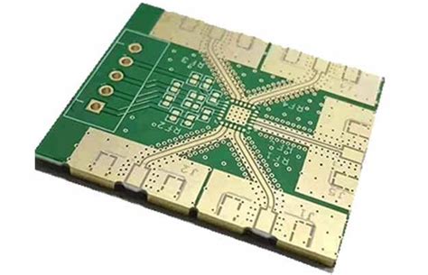
The Role of PCB Layout in High-Speed Signal Performance
In the realm of high-speed signal design, the role of printed circuit board (PCB) layout cannot be overstated. As electronic devices continue to evolve, the demand for faster data transmission rates has surged, necessitating meticulous attention to PCB layout to ensure optimal signal integrity and performance. The intricate interplay between signal speed and PCB design elements underscores the importance of understanding how various factors influence high-speed signal behavior.
To begin with, the physical layout of a PCB significantly impacts signal integrity.
High-speed signals are particularly susceptible to issues such as signal reflection, crosstalk, and electromagnetic interference (EMI). These phenomena can degrade signal quality, leading to data corruption and system malfunctions. Therefore, careful consideration of trace routing, layer stacking, and component placement is essential. For instance, maintaining consistent trace impedance is crucial to minimize signal reflections. This can be achieved by controlling trace width, spacing, and the dielectric properties of the PCB material.
Moreover, the concept of controlled impedance is pivotal in high-speed PCB design.
Controlled impedance ensures that the characteristic impedance of a transmission line remains constant along its length, thereby reducing signal reflections and maintaining signal integrity. This is particularly important for differential pairs, which are commonly used in high-speed designs to mitigate noise and EMI. Differential pairs require precise matching of trace lengths and spacing to ensure that the signals remain in phase and maintain their integrity.
Transitioning to the topic of signal routing, it is imperative to minimize the length of high-speed signal traces.
Longer traces introduce greater inductance and capacitance, which can distort the signal and increase the likelihood of crosstalk. Additionally, avoiding sharp corners in trace routing is advisable, as these can cause impedance discontinuities and signal reflections. Instead, using smooth, gradual bends helps maintain consistent impedance and signal quality.
Another critical aspect of PCB layout in high-speed signal design is the use of ground planes.
Ground planes provide a low-impedance return path for high-speed signals, reducing the potential for EMI and crosstalk. They also help to stabilize the reference voltage, which is essential for maintaining signal integrity. Ensuring that ground planes are continuous and free of gaps is vital, as discontinuities can disrupt the return path and degrade signal performance.
Furthermore, the placement of decoupling capacitors plays a significant role in high-speed PCB design.
Decoupling capacitors help to filter out noise and provide a stable power supply to high-speed components. Placing these capacitors as close as possible to the power pins of integrated circuits (ICs) minimizes the inductance of the power delivery network, thereby enhancing signal integrity.
In addition to these considerations, the choice of PCB materials also influences high-speed signal performance.
Materials with low dielectric constant and low loss tangent are preferred for high-speed designs, as they reduce signal attenuation and dispersion. High-frequency laminates, such as those made from polytetrafluoroethylene (PTFE) or other advanced composites, are often used to achieve superior signal performance.
In conclusion, the role of PCB layout in high-speed signal performance is multifaceted and demands a comprehensive understanding of various design principles. From controlled impedance and trace routing to ground planes and decoupling capacitors, each element plays a crucial part in ensuring signal integrity and optimal performance. As technology continues to advance, the importance of meticulous PCB layout in high-speed signal design will only grow, underscoring the need for designers to stay abreast of best practices and emerging trends in this critical field.
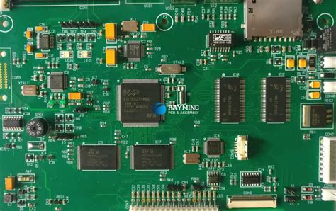
Best Practices for High-Speed Signal Routing
High-speed signal design is a critical aspect of modern electronic systems, where the integrity and performance of signals are paramount. To ensure optimal functionality, it is essential to adhere to best practices for high-speed signal routing. These practices help mitigate issues such as signal degradation, crosstalk, and electromagnetic interference (EMI), which can significantly impact the performance of high-speed circuits.
One of the fundamental principles in high-speed signal routing is maintaining signal integrity.
This involves ensuring that the signal path is as short and direct as possible. Long traces can introduce delays and increase the likelihood of signal reflections, which can distort the signal. To minimize these effects, designers should use controlled impedance traces, which help maintain a consistent impedance along the signal path. This consistency is crucial for preventing signal reflections and ensuring that the signal reaches its destination without degradation.
In addition to controlled impedance, proper termination is essential for high-speed signal routing.
Termination resistors can be used to match the impedance of the signal source and the load, thereby reducing reflections. There are several termination techniques, including series, parallel, and Thevenin termination, each with its own advantages and applications. Selecting the appropriate termination method depends on the specific requirements of the circuit and the characteristics of the signal.
Another critical aspect of high-speed signal routing is minimizing crosstalk between adjacent signal traces.
Crosstalk occurs when a signal on one trace induces an unwanted signal on a neighboring trace, leading to potential data corruption. To mitigate crosstalk, designers should maintain adequate spacing between high-speed traces and use differential pairs where possible. Differential signaling involves using two complementary signals, which helps cancel out noise and reduces susceptibility to crosstalk. Additionally, routing high-speed signals on different layers with a ground plane in between can further isolate them and minimize interference.
Electromagnetic interference (EMI) is another challenge in high-speed signal design.
EMI can be generated by high-speed signals and can affect the performance of other components in the system. To reduce EMI, designers should use proper grounding techniques and ensure that the return path for high-speed signals is as short and direct as possible. A solid ground plane is highly effective in providing a low-impedance return path and reducing EMI. Furthermore, using decoupling capacitors near high-speed components can help filter out high-frequency noise and stabilize the power supply.
Via placement is also a crucial consideration in high-speed signal routing.
Vias are used to connect traces on different layers of a printed circuit board (PCB), but they can introduce inductance and capacitance, which can affect signal integrity. To minimize these effects, designers should use as few vias as possible and ensure that the vias are properly placed. When routing differential pairs, it is important to keep the vias symmetrical to maintain the balance of the differential signals.
Lastly, signal routing should be carefully planned to avoid unnecessary bends and corners.
Sharp bends can cause impedance discontinuities and signal reflections. Instead, designers should use smooth, gradual curves or 45-degree angles when routing high-speed traces. This practice helps maintain signal integrity and reduces the risk of signal degradation.
In conclusion, high-speed signal routing requires careful consideration of various factors to ensure signal integrity and optimal performance. By adhering to best practices such as maintaining controlled impedance, proper termination, minimizing crosstalk, reducing EMI, careful via placement, and avoiding sharp bends, designers can effectively manage the challenges associated with high-speed signal design. These practices are essential for the development of reliable and efficient electronic systems in today’s fast-paced technological landscape.