Flex pcb layout guidelines
Best Practices For Flex PCB Layout Design
When designing flexible printed circuit boards (flex PCBs), adhering to best practices is crucial to ensure reliability, performance, and manufacturability. Flex PCBs offer unique advantages, such as the ability to bend and twist, making them ideal for applications where space constraints and mechanical flexibility are paramount. However, these benefits come with specific design challenges that must be addressed through meticulous planning and execution.
To begin with, understanding the material properties of flex PCBs is essential.
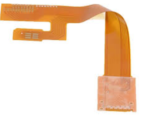
Unlike rigid PCBs, flex circuits are made from flexible substrates like polyimide, which can endure bending and flexing. This flexibility, however, necessitates careful consideration of the mechanical stresses that the board will encounter. Therefore, it is advisable to avoid sharp bends and instead use gradual curves with a minimum bend radius. Typically, a bend radius of at least ten times the thickness of the flex PCB is recommended to prevent stress fractures and maintain the integrity of the circuit.
Moreover, trace layout plays a significant role in the durability and functionality of flex PCBs.
Traces should be routed perpendicular to the bend lines rather than parallel to minimize stress concentration. Additionally, using curved traces instead of sharp angles can further reduce stress points. It is also beneficial to stagger traces on different layers to avoid creating weak spots that could lead to cracking or delamination.
Another critical aspect is the stack-up configuration.
Flex PCBs can be single-sided, double-sided, or multilayered, and each configuration has its own set of guidelines. For multilayer flex PCBs, it is important to balance the copper distribution across layers to prevent warping. Symmetrical stack-ups are preferred as they provide uniform mechanical properties and reduce the risk of twisting or bowing during fabrication and operation.
Furthermore, the choice of coverlay material and its application is vital.
Coverlay, typically made from polyimide, protects the flex PCB from environmental factors and mechanical wear. Ensuring that the coverlay is properly aligned and free from air bubbles or wrinkles is crucial for maintaining the board’s reliability. Additionally, the use of stiffeners in areas that require additional support, such as connector interfaces, can enhance the mechanical robustness of the flex PCB.
Thermal management is another important consideration in flex PCB design.
Flexible circuits often operate in environments with varying temperatures, and excessive heat can lead to material degradation and failure. Therefore, incorporating thermal reliefs and ensuring adequate heat dissipation through proper layout and material selection is essential. Utilizing thermal vias and strategically placing components to distribute heat evenly can help mitigate thermal issues.
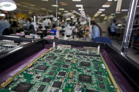
In addition to these technical considerations, collaboration with the manufacturer during the design phase can significantly improve the outcome.
Manufacturers can provide valuable insights into the limitations and capabilities of their fabrication processes, allowing designers to make informed decisions that align with manufacturing constraints. This collaboration can also help identify potential issues early in the design process, reducing the likelihood of costly revisions and delays.
In conclusion, designing flex PCBs requires a comprehensive understanding of material properties, mechanical stresses, trace layout, stack-up configuration, coverlay application, and thermal management. By following these best practices and maintaining close communication with the manufacturer, designers can create reliable, high-performance flex PCBs that meet the demands of modern electronic applications. The meticulous attention to detail in each aspect of the design process ensures that the final product not only functions as intended but also withstands the rigors of its operating environment.
Common Mistakes To Avoid In Flex PCB Layout
When designing a flexible printed circuit board (flex PCB), it is crucial to be aware of common mistakes that can compromise the functionality and reliability of the final product. One of the most frequent errors is neglecting to account for the mechanical stresses that the flex PCB will endure. Unlike rigid PCBs, flex PCBs are designed to bend and flex, which means that the layout must accommodate these movements. Failing to do so can lead to cracked traces, delamination, and ultimately, circuit failure. Therefore, it is essential to incorporate bend radii and avoid placing vias and components in areas that will experience significant flexing.
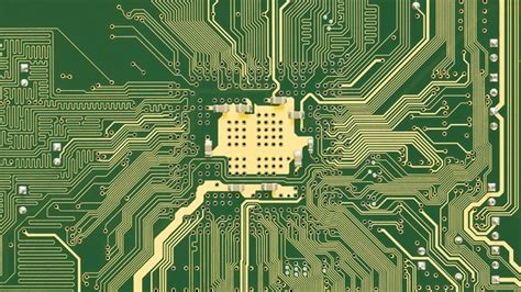
Another common mistake is improper trace routing.
In flex PCBs, traces should be routed in a manner that minimizes stress. For instance, traces should be routed perpendicular to the bend lines rather than parallel. This reduces the likelihood of trace cracking when the board is bent. Additionally, using curved traces instead of sharp angles can help distribute mechanical stress more evenly, further enhancing the durability of the flex PCB.
Moreover, designers often overlook the importance of material selection.
The choice of substrate and adhesive materials can significantly impact the performance of a flex PCB. Materials with poor flexibility or inadequate thermal properties can lead to issues such as warping, delamination, and thermal expansion mismatches. It is advisable to consult with material suppliers and consider the specific environmental conditions the flex PCB will be exposed to, such as temperature extremes and humidity, to select the most appropriate materials.
Thermal management is another critical aspect that is sometimes neglected.
Flex PCBs can be more susceptible to thermal issues due to their thinner and more flexible nature. Inadequate thermal management can result in overheating, which can degrade the performance of the components and the board itself. To mitigate this, designers should consider incorporating thermal vias, heat sinks, and appropriate trace widths to ensure efficient heat dissipation.
Furthermore, insufficient attention to the stack-up design can lead to performance issues.
The stack-up determines the arrangement of the various layers in a flex PCB, including signal, power, and ground layers. An improper stack-up can result in signal integrity problems, such as crosstalk and electromagnetic interference (EMI). Ensuring a well-balanced stack-up with adequate spacing between layers and proper grounding can help maintain signal integrity and reduce EMI.
Additionally, designers often make the mistake of not performing thorough design rule checks (DRCs) and simulations.
DRCs can help identify potential issues such as spacing violations, trace width errors, and other design rule violations that could compromise the functionality of the flex PCB. Simulations, on the other hand, can provide insights into the electrical and thermal performance of the design, allowing for adjustments before the manufacturing stage.
Lastly, inadequate documentation and communication with the manufacturer can lead to production issues.
Providing detailed documentation, including assembly drawings, material specifications, and testing requirements, is essential for ensuring that the manufacturer understands the design intent and can produce the flex PCB accurately. Clear communication can help avoid misunderstandings and ensure that the final product meets the desired specifications.
In conclusion, avoiding these common mistakes in flex PCB layout requires careful consideration of mechanical stresses, trace routing, material selection, thermal management, stack-up design, thorough design rule checks, and effective communication with the manufacturer. By addressing these factors, designers can enhance the reliability and performance of their flex PCBs, ensuring they meet the demands of their intended applications.
Material Selection Tips For Flex PCB Layout
When designing a flexible printed circuit board (flex PCB), material selection is a critical aspect that significantly influences the performance, reliability, and manufacturability of the final product. The unique properties of flex PCBs, such as their ability to bend and twist, necessitate careful consideration of the materials used in their construction. To ensure optimal functionality and longevity, it is essential to follow specific guidelines when selecting materials for flex PCB layouts.
First and foremost, the choice of substrate material is paramount.
Polyimide is the most commonly used substrate for flex PCBs due to its excellent thermal stability, mechanical strength, and flexibility. Polyimide can withstand high temperatures, making it suitable for applications that require soldering and other heat-intensive processes. Additionally, its mechanical properties allow the flex PCB to endure repeated bending and flexing without cracking or breaking. However, it is important to note that polyimide is relatively expensive compared to other materials, so cost considerations should be balanced with performance requirements.
In addition to the substrate, the selection of adhesive materials is equally important.
Adhesives are used to bond the various layers of the flex PCB together, and their properties can significantly impact the board’s flexibility and durability. Acrylic-based adhesives are commonly used due to their excellent flexibility and strong bonding capabilities. They can maintain their adhesive properties over a wide temperature range, ensuring the integrity of the flex PCB in various environmental conditions. However, for applications requiring higher thermal resistance, epoxy-based adhesives may be more suitable, despite being less flexible than acrylics.
The choice of conductive materials for the flex PCB’s traces and pads is another crucial consideration.
Copper is the preferred material for conductive traces due to its excellent electrical conductivity and ductility. Copper can be easily etched into fine patterns, allowing for high-density circuit designs. However, the thickness of the copper layer must be carefully controlled to balance flexibility and electrical performance. Thinner copper layers enhance flexibility but may increase electrical resistance, while thicker layers improve conductivity but reduce the board’s ability to bend.
Furthermore, the selection of coverlay materials, which protect the conductive traces and provide insulation, is vital for the flex PCB’s reliability.
Polyimide coverlays are commonly used due to their compatibility with polyimide substrates and their ability to withstand high temperatures. They provide excellent mechanical protection and electrical insulation, ensuring the flex PCB’s longevity. However, for applications requiring enhanced flexibility, liquid photoimageable (LPI) solder masks may be considered as an alternative to traditional coverlays. LPI solder masks offer good flexibility and can be precisely applied to intricate circuit patterns.
Moreover, it is essential to consider the environmental conditions in which the flex PCB will operate.
Factors such as temperature, humidity, and exposure to chemicals can affect the performance and lifespan of the materials used. For instance, in high-humidity environments, materials with low moisture absorption rates should be selected to prevent degradation and ensure reliable operation. Similarly, for applications involving exposure to harsh chemicals, materials with high chemical resistance should be chosen to maintain the integrity of the flex PCB.
In conclusion, material selection for flex PCB layouts requires a comprehensive understanding of the properties and performance characteristics of various materials. By carefully considering factors such as substrate, adhesive, conductive materials, coverlay, and environmental conditions, designers can ensure the development of robust and reliable flex PCBs. Adhering to these guidelines will not only enhance the performance and durability of the flex PCB but also contribute to the overall success of the electronic device in which it is employed.
Advanced Techniques For Optimizing Flex PCB Layout
Flex PCB layout design is a sophisticated process that requires meticulous attention to detail and a deep understanding of the unique properties of flexible circuits. To optimize the layout of a flex PCB, it is essential to consider several advanced techniques that can significantly enhance performance, reliability, and manufacturability
One of the primary considerations in flex PCB design is the minimization of mechanical stress.
Flex circuits are often subjected to bending, folding, and twisting, which can lead to mechanical fatigue and eventual failure. To mitigate these risks, designers should employ curved traces instead of sharp angles, as sharp corners can concentrate stress and become potential points of failure. Additionally, staggered vias and teardrop-shaped pads can help distribute mechanical stress more evenly across the circuit.
Another critical aspect of optimizing flex PCB layout is the careful management of signal integrity.
High-speed signals can be particularly challenging to route on a flexible substrate due to the potential for signal degradation and electromagnetic interference. To address these issues, designers should use controlled impedance traces and maintain consistent trace widths and spacing. Furthermore, incorporating ground planes and shielding can help reduce noise and crosstalk, ensuring that signal integrity is maintained even in demanding applications.
Thermal management is also a crucial factor in flex PCB design.
Flexible circuits are often used in compact and densely populated electronic assemblies, where heat dissipation can be a significant concern. To enhance thermal performance, designers should consider using thicker copper layers and incorporating thermal vias to facilitate heat transfer away from critical components. Additionally, strategic placement of heat-generating components and the use of thermal reliefs can help manage temperature distribution across the flex PCB.
Material selection plays a pivotal role in the performance and reliability of flex PCBs.
Polyimide is a commonly used substrate material due to its excellent thermal stability, mechanical flexibility, and chemical resistance. However, other materials such as polyester and liquid crystal polymer (LCP) may be more suitable for specific applications. Designers should carefully evaluate the material properties and select the most appropriate substrate based on the intended use and environmental conditions.
Design for manufacturability (DFM) is another essential consideration in flex PCB layout.
To ensure that the design can be efficiently and cost-effectively manufactured, designers should adhere to industry standards and guidelines. This includes maintaining appropriate trace widths and spacing, avoiding overly complex routing, and ensuring that the design can be easily assembled and tested. Collaboration with manufacturing partners during the design phase can help identify potential issues and optimize the layout for production.
In addition to these technical considerations, it is important to leverage advanced design tools and software to streamline the flex PCB layout process.
Modern CAD tools offer a range of features specifically tailored for flex circuit design, including automated routing, impedance calculation, and 3D visualization. By utilizing these tools, designers can more effectively manage the complexities of flex PCB layout and achieve optimal results.
In conclusion, optimizing flex PCB layout requires a comprehensive approach that addresses mechanical stress, signal integrity, thermal management, material selection, and manufacturability. By employing advanced techniques and leveraging modern design tools, designers can create flexible circuits that meet the demanding requirements of today’s electronic applications. Through careful planning and attention to detail, it is possible to achieve a high-performance, reliable, and manufacturable flex PCB design.