Flex pcb layer stackup
Understanding The Basics Of Flex PCB Layer Stackup
Flex PCB layer stackup is a critical aspect of designing flexible printed circuit boards, which are increasingly used in modern electronics due to their versatility and ability to conform to complex shapes. Understanding the basics of flex PCB layer stackup is essential for engineers and designers aiming to optimize the performance and reliability of their electronic devices.
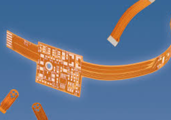
To begin with, a flex PCB, or flexible printed circuit board, is a type of PCB that can bend and flex, unlike traditional rigid PCBs.
This flexibility is achieved through the use of flexible base materials such as polyimide or polyester films, which provide the necessary mechanical properties. The layer stackup of a flex PCB refers to the arrangement and sequence of conductive and insulating layers that make up the board. This stackup is crucial because it directly impacts the electrical performance, mechanical durability, and manufacturability of the flex PCB.
One of the fundamental components of a flex PCB layer stackup is the conductive layer, typically made of copper.
Copper layers are responsible for carrying electrical signals and power throughout the circuit. Depending on the design requirements, a flex PCB can have multiple copper layers, which are separated by insulating layers. These insulating layers, often made of polyimide, provide electrical isolation between the conductive layers and contribute to the overall flexibility of the PCB.
In addition to the conductive and insulating layers, a flex PCB stackup may also include adhesive layers.
These adhesive layers bond the various layers together, ensuring structural integrity. The choice of adhesive material is important, as it must provide strong adhesion while maintaining flexibility and thermal stability. Common adhesive materials include acrylic and epoxy-based adhesives.
Moreover, the layer stackup of a flex PCB can be classified into different types based on the number of layers and their arrangement.
Single-sided flex PCBs have one conductive layer on a flexible substrate, making them simple and cost-effective. Double-sided flex PCBs have two conductive layers, one on each side of the substrate, allowing for more complex routing and increased functionality. Multilayer flex PCBs, on the other hand, consist of multiple conductive and insulating layers stacked together, enabling even more intricate designs and higher circuit density.
Transitioning to the design considerations, it is essential to carefully plan the layer stackup to achieve the desired electrical and mechanical performance.
For instance, the thickness of the copper layers must be chosen based on the current-carrying capacity and signal integrity requirements. Thicker copper layers can handle higher currents but may reduce flexibility. Similarly, the thickness and material properties of the insulating layers must be selected to provide adequate electrical isolation while maintaining the desired level of flexibility.
Furthermore, the arrangement of the layers in the stackup can significantly impact the overall performance of the flex PCB.
For example, placing ground and power planes close to signal layers can help reduce electromagnetic interference (EMI) and improve signal integrity. Additionally, symmetrical stackups, where the layers are arranged symmetrically around the central axis, can help minimize mechanical stress and prevent warping during manufacturing and operation.
In conclusion, understanding the basics of flex PCB layer stackup is vital for designing reliable and high-performance flexible circuits. By carefully selecting and arranging the conductive, insulating, and adhesive layers, designers can optimize the electrical and mechanical properties of the flex PCB to meet the specific requirements of their applications. As the demand for flexible electronics continues to grow, mastering the intricacies of flex PCB layer stackup will become increasingly important for engineers and designers in the field.
Key Considerations For Designing Flex PCB Layer Stackup
When designing a flex PCB layer stackup, several key considerations must be taken into account to ensure optimal performance and reliability. One of the primary factors to consider is the material selection. Flex PCBs typically use polyimide as the base material due to its excellent thermal stability, flexibility, and dielectric properties. However, the choice of adhesive and coverlay materials is equally important, as these components must withstand the mechanical stresses and environmental conditions the PCB will encounter.
Another critical aspect is the layer configuration.
The number of layers in a flex PCB can vary depending on the complexity of the circuit and the space constraints. Single-layer flex PCBs are simpler and less expensive but may not provide the necessary routing options for more complex designs. Multi-layer flex PCBs, on the other hand, offer greater design flexibility but require careful consideration of signal integrity and impedance control. It is essential to balance the need for additional layers with the potential increase in manufacturing complexity and cost.
Signal integrity is a crucial consideration in flex PCB design.
High-speed signals can be particularly susceptible to issues such as crosstalk, signal attenuation, and electromagnetic interference (EMI). To mitigate these problems, designers must carefully plan the stackup to include appropriate ground and power planes. These planes help to provide a stable reference for signals and reduce the potential for noise and interference. Additionally, controlled impedance traces may be necessary to ensure signal integrity, particularly in high-frequency applications.
Thermal management is another important factor in flex PCB design.
The flexible nature of these PCBs can make them more susceptible to thermal expansion and contraction, which can lead to mechanical stress and potential failure. To address this, designers should consider the thermal properties of the materials used and incorporate features such as thermal vias and heat sinks to dissipate heat effectively. Proper thermal management ensures the longevity and reliability of the flex PCB in various operating conditions.
Mechanical considerations also play a significant role in flex PCB layer stackup design.
The bending and flexing of the PCB can introduce mechanical stress, which can affect the performance and durability of the circuit. To minimize these stresses, designers should optimize the bend radius and avoid sharp bends or folds. Additionally, the placement of components and traces should be carefully planned to prevent stress concentration in critical areas. Reinforcement materials, such as stiffeners, can also be used to provide additional support and reduce mechanical strain.
Manufacturability is a key consideration that cannot be overlooked.
The design of the flex PCB layer stackup must be compatible with the manufacturing processes and capabilities of the chosen fabricator. This includes considerations such as minimum trace width and spacing, via sizes, and the overall thickness of the PCB. Collaborating with the manufacturer early in the design process can help identify potential issues and ensure that the final design is both manufacturable and cost-effective.
In conclusion, designing a flex PCB layer stackup involves a careful balance of material selection, layer configuration, signal integrity, thermal management, mechanical considerations, and manufacturability. By addressing these key factors, designers can create flex PCBs that meet the performance, reliability, and cost requirements of their applications. The complexity of flex PCB design necessitates a thorough understanding of these considerations to achieve a successful and robust final product.
Common Challenges In Flex PCB Layer Stackup And How To Overcome Them
Flex PCB layer stackup is a critical aspect of designing flexible printed circuit boards, which are increasingly used in various applications due to their versatility and ability to conform to complex shapes. However, the process of creating an effective flex PCB layer stackup is fraught with challenges that can impact the performance, reliability, and manufacturability of the final product. Understanding these common challenges and how to overcome them is essential for engineers and designers working in this field.
One of the primary challenges in flex PCB layer stackup is managing the mechanical stress that the board will experience during its lifecycle.
Flex PCBs are often subjected to bending, twisting, and other forms of mechanical deformation, which can lead to issues such as delamination, cracking, or even complete failure of the circuit. To mitigate these risks, it is crucial to carefully select materials that offer the right balance of flexibility and durability. Polyimide is a popular choice for flex PCBs due to its excellent thermal stability and mechanical properties. Additionally, incorporating strain relief features, such as curved traces and filleted corners, can help distribute mechanical stress more evenly across the board.
Another significant challenge is ensuring signal integrity in high-speed applications.
Flex PCBs are often used in environments where maintaining signal integrity is critical, such as in telecommunications and medical devices. The flexible nature of these boards can introduce variations in impedance, which can lead to signal degradation and increased electromagnetic interference (EMI). To address this issue, designers must pay close attention to the stackup configuration, ensuring that the dielectric materials and trace widths are carefully controlled to maintain consistent impedance. Utilizing ground planes and shielding techniques can also help minimize EMI and improve overall signal integrity.
Thermal management is another area where flex PCB layer stackup can present challenges.
Flexible circuits are often used in compact, high-density applications where heat dissipation can be a concern. The thin and flexible nature of these boards can make it difficult to manage heat effectively, leading to potential overheating and reduced reliability. To overcome this challenge, designers can incorporate thermal vias and heat spreaders into the stackup to facilitate better heat dissipation. Additionally, selecting materials with high thermal conductivity and optimizing the layout to minimize hotspots can further enhance thermal management.
Manufacturability is a critical consideration in flex PCB layer stackup design.
The unique properties of flexible circuits can complicate the manufacturing process, leading to potential issues such as misalignment, warping, and difficulties in handling. To ensure a smooth manufacturing process, it is essential to work closely with experienced fabricators who understand the nuances of flex PCB production. Designing with manufacturability in mind, such as incorporating alignment features and specifying appropriate tolerances, can help minimize production challenges and improve yield.
In conclusion, while flex PCB layer stackup presents several challenges, understanding these issues and implementing effective strategies can lead to successful designs that meet the demands of modern applications. By carefully selecting materials, managing mechanical stress, ensuring signal integrity, addressing thermal management, and considering manufacturability, designers can overcome these challenges and create reliable, high-performance flexible circuits. As the demand for flexible electronics continues to grow, mastering the intricacies of flex PCB layer stackup will become increasingly important for engineers and designers in this evolving field.
Innovations And Trends In Flex PCB Layer Stackup Technology
Flex PCB layer stackup technology has undergone significant advancements in recent years, driven by the increasing demand for more compact, reliable, and versatile electronic devices. As the electronics industry continues to evolve, innovations in flex PCB layer stackup are playing a crucial role in meeting the stringent requirements of modern applications. These advancements are not only enhancing the performance and durability of flexible printed circuit boards but also expanding their potential uses across various sectors.
One of the most notable trends in flex PCB layer stackup technology is the development of multi-layer flex PCBs.
Traditionally, flex PCBs were limited to single or double layers, which restricted their functionality and application scope. However, with the advent of multi-layer flex PCBs, designers can now incorporate more complex circuitry within a smaller footprint. This innovation has been particularly beneficial for industries such as aerospace, medical devices, and consumer electronics, where space constraints and high performance are critical.
In addition to multi-layer designs, the use of advanced materials has significantly impacted flex PCB layer stackup technology.
Polyimide, for instance, has become a popular choice due to its excellent thermal stability, mechanical strength, and flexibility. This material allows for the creation of thinner and more robust flex PCBs, which can withstand harsh environmental conditions and mechanical stress. Moreover, the integration of advanced adhesives and bonding techniques has further improved the reliability and longevity of these flexible circuits.
Another key innovation in flex PCB layer stackup technology is the incorporation of rigid-flex designs.
Rigid-flex PCBs combine the benefits of both rigid and flexible circuits, offering enhanced mechanical stability and design flexibility. This hybrid approach allows for more efficient use of space and can reduce the overall weight of the electronic assembly. Consequently, rigid-flex PCBs are increasingly being adopted in applications where both flexibility and rigidity are required, such as in wearable devices and automotive electronics.
Furthermore, advancements in manufacturing processes have played a pivotal role in the evolution of flex PCB layer stackup technology.
Techniques such as laser drilling and precision etching have enabled the production of finer and more intricate circuit patterns. These processes allow for higher density interconnects and improved signal integrity, which are essential for high-speed and high-frequency applications. Additionally, the use of automated optical inspection (AOI) and other quality control measures ensures that the final products meet the highest standards of reliability and performance.
The trend towards miniaturization in electronics has also influenced flex PCB layer stackup technology.
As devices become smaller and more compact, the need for thinner and more flexible PCBs has increased. Innovations such as ultra-thin laminates and microvia technology have addressed this demand, enabling the production of highly compact and lightweight flex PCBs. These advancements have opened up new possibilities for the design and development of next-generation electronic devices.
In conclusion, the continuous innovations and trends in flex PCB layer stackup technology are driving the electronics industry towards new heights of performance and reliability. The development of multi-layer designs, advanced materials, rigid-flex configurations, and cutting-edge manufacturing processes are all contributing to the enhanced capabilities of flexible printed circuit boards. As the demand for more compact, efficient, and versatile electronic devices grows, the importance of these technological advancements cannot be overstated. The future of flex PCB layer stackup technology promises even greater innovations, paving the way for more sophisticated and high-performing electronic solutions.