Print a circuit board
Evolution Of Printed Wiring Boards: From Inception To Modern Applications
The evolution of printed wiring boards (PWBs) is a fascinating journey that reflects the broader technological advancements of the 20th and 21st centuries. Initially conceived as a means to simplify the complex wiring systems in electronic devices, PWBs have undergone significant transformations, both in terms of design and functionality. The inception of printed wiring boards can be traced back to the early 20th century when the burgeoning field of electronics demanded more efficient methods of connecting components. Before PWBs, electronic circuits were constructed using point-to-point wiring, a labor-intensive process prone to errors and inconsistencies. The introduction of PWBs revolutionized this process by providing a standardized platform for mounting and interconnecting electronic components.
As the demand for more compact and reliable electronic devices grew, so did the need for more sophisticated PWBs.
The mid-20th century saw the development of double-sided and multilayer boards, which allowed for more complex circuits to be accommodated within a smaller footprint. This advancement was crucial in the miniaturization of electronic devices, paving the way for the development of modern computers, telecommunications equipment, and consumer electronics. The ability to stack multiple layers of circuitry within a single board not only increased the functionality of electronic devices but also enhanced their reliability by reducing the number of physical connections that could potentially fail.
Transitioning into the late 20th century, the rise of surface mount technology (SMT) marked another significant milestone in the evolution of PWBs.
SMT allowed components to be mounted directly onto the surface of the board, eliminating the need for drilled holes and further reducing the size and weight of electronic assemblies. This innovation was particularly important in the development of portable electronic devices, such as laptops and mobile phones, which require high-density circuitry in a compact form factor. Moreover, SMT improved the performance of electronic devices by minimizing the length of electrical paths, thereby reducing signal delay and power consumption.
In recent years, the evolution of printed wiring boards has been driven by the increasing complexity and performance demands of modern electronic applications.
The advent of high-speed digital circuits, for instance, has necessitated the development of advanced materials and manufacturing techniques to ensure signal integrity and thermal management. Innovations such as flexible and rigid-flex PWBs have emerged to meet the needs of applications that require dynamic bending and folding, such as wearable technology and aerospace systems. These flexible boards offer unique advantages in terms of weight reduction and design versatility, enabling engineers to create more innovative and ergonomic products.
Furthermore, the integration of advanced manufacturing technologies, such as additive manufacturing and laser direct structuring, is poised to redefine the future of printed wiring boards.
These techniques offer the potential for greater design freedom, reduced material waste, and faster prototyping, which are essential in today’s fast-paced electronics industry. As the Internet of Things (IoT) and artificial intelligence (AI) continue to expand, the demand for more intelligent and interconnected devices will drive further innovations in PWB technology.
In conclusion, the evolution of printed wiring boards from their inception to modern applications is a testament to the relentless pursuit of efficiency and innovation in the electronics industry. As technology continues to advance, PWBs will undoubtedly play a crucial role in shaping the future of electronic devices, enabling new possibilities and applications that were once unimaginable.
Key Materials And Technologies In Printed Wiring Board Manufacturing
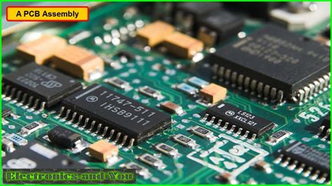
Printed wiring boards (PWBs), commonly known as printed circuit boards (PCBs), are integral components in modern electronic devices, serving as the foundation for mounting and interconnecting electronic components. The manufacturing of PWBs involves a complex interplay of materials and technologies, each contributing to the board’s functionality, reliability, and performance. Understanding these key materials and technologies is essential for appreciating the intricacies of PWB manufacturing.
At the core of PWB manufacturing is the substrate material, which provides the structural support for the board.
The most commonly used substrate is a composite material known as FR-4, which consists of woven fiberglass cloth with an epoxy resin binder. This material is favored for its excellent mechanical strength, thermal resistance, and electrical insulation properties. However, as electronic devices become more sophisticated, there is a growing demand for substrates with enhanced thermal management capabilities. Consequently, materials such as metal-core PCBs, which incorporate a metal layer to dissipate heat, are gaining popularity in applications requiring superior thermal performance.
In addition to the substrate, the conductive material used to form the circuit traces is crucial.
Copper is the predominant choice due to its excellent electrical conductivity and ease of etching. The copper is typically laminated onto the substrate in thin sheets and then patterned through a series of photolithographic and etching processes to create the desired circuit layout. As electronic devices continue to shrink in size, the need for finer circuit traces has led to advancements in photolithography techniques, enabling the production of high-density interconnect (HDI) boards with microvias and finer lines.
The solder mask is another essential material in PWB manufacturing.
This protective layer, usually made of a polymer-based compound, is applied over the copper traces to prevent oxidation and short circuits. It also provides a surface for soldering components onto the board. The choice of solder mask material can impact the board’s thermal and chemical resistance, making it a critical consideration in the manufacturing process.
Furthermore, the surface finish applied to the copper pads is vital for ensuring reliable soldering and long-term performance.
Common surface finishes include hot air solder leveling (HASL), electroless nickel immersion gold (ENIG), and immersion silver. Each finish offers distinct advantages and trade-offs in terms of solderability, shelf life, and cost. For instance, ENIG is favored for its excellent surface planarity and corrosion resistance, making it suitable for fine-pitch components and high-reliability applications.
As technology advances, emerging materials and technologies are continually reshaping the PWB manufacturing landscape.
For example, the integration of flexible and rigid-flex PCBs is becoming increasingly prevalent, driven by the demand for lightweight and compact electronic devices. These boards utilize flexible substrates, such as polyimide, allowing them to bend and conform to various shapes, thus enabling innovative design possibilities.
Moreover, the advent of additive manufacturing techniques, such as inkjet and 3D printing, is poised to revolutionize PWB production.
These technologies offer the potential for rapid prototyping and customization, reducing lead times and material waste. As these methods mature, they may complement or even replace traditional subtractive manufacturing processes in certain applications.
In conclusion, the manufacturing of printed wiring boards is a dynamic field characterized by a diverse array of materials and technologies. From the choice of substrate and conductive materials to the application of surface finishes and protective layers, each element plays a pivotal role in determining the board’s performance and reliability. As the demand for more advanced and compact electronic devices continues to grow, ongoing innovations in materials and manufacturing techniques will undoubtedly shape the future of PWB production.
Environmental Impact And Sustainability Practices In Printed Wiring Board Production
Printed wiring boards (PWBs), commonly known as printed circuit boards (PCBs), are integral components in modern electronic devices, serving as the foundation for mounting and interconnecting electronic components. As the demand for electronic devices continues to rise, the environmental impact of PWB production has become a significant concern. The manufacturing process involves various materials and chemicals, which, if not managed properly, can lead to environmental degradation. Consequently, the industry is increasingly focusing on sustainability practices to mitigate these impacts.
The production of PWBs involves several stages, including substrate preparation, patterning, etching, and plating.
Each of these stages can contribute to environmental issues. For instance, the etching process, which removes unwanted copper from the board, often uses chemicals like ferric chloride or ammonium persulfate. These chemicals, if not disposed of correctly, can contaminate water sources and harm aquatic life. Additionally, the energy-intensive nature of PWB manufacturing contributes to greenhouse gas emissions, further exacerbating environmental concerns.
In response to these challenges, the industry is adopting various sustainability practices.
One such practice is the implementation of closed-loop systems for chemical management. By recycling and reusing chemicals within the production process, manufacturers can significantly reduce waste and minimize the risk of environmental contamination. Moreover, advancements in technology have led to the development of alternative, less harmful chemicals for use in the etching and plating processes, thereby reducing the ecological footprint of PWB production.
Energy efficiency is another critical area of focus. Manufacturers are increasingly investing in energy-efficient machinery and processes to lower their carbon footprint.
For example, the use of advanced imaging technologies in the patterning stage can reduce energy consumption by minimizing the need for multiple processing steps. Additionally, some companies are exploring the use of renewable energy sources, such as solar or wind power, to further decrease their reliance on fossil fuels.
Material selection also plays a vital role in enhancing the sustainability of PWB production.
The industry is moving towards the use of environmentally friendly materials, such as lead-free solders and halogen-free laminates, which reduce the release of toxic substances during manufacturing and disposal. Furthermore, the adoption of biodegradable substrates is being explored as a means to address the issue of electronic waste, which poses a significant environmental challenge due to the non-biodegradable nature of traditional PWB materials.
Collaboration across the supply chain is essential for driving sustainability in PWB production.
Manufacturers, suppliers, and customers are increasingly working together to establish standards and best practices that promote environmental responsibility. Industry associations and regulatory bodies are also playing a crucial role by setting guidelines and encouraging compliance with environmental regulations.
In conclusion, while the production of printed wiring boards presents several environmental challenges, the industry is making strides towards sustainability through innovative practices and technologies. By focusing on chemical management, energy efficiency, material selection, and collaborative efforts, the PWB industry is taking significant steps to reduce its environmental impact. As these practices continue to evolve, they hold the promise of not only minimizing the ecological footprint of PWB production but also setting a precedent for sustainability in the broader electronics manufacturing sector.
Innovations In Printed Wiring Board Design For Enhanced Performance
Printed wiring boards (PWBs), often referred to as printed circuit boards (PCBs), are the backbone of modern electronic devices, providing the necessary mechanical support and electrical connections for various components. As technology continues to advance at a rapid pace, innovations in PWB design have become crucial for enhancing the performance and reliability of electronic systems. These innovations are driven by the increasing demand for miniaturization, higher functionality, and improved thermal management in electronic devices.
One of the most significant advancements in PWB design is the development of high-density interconnect (HDI) technology.
HDI boards are characterized by their finer lines and spaces, smaller vias, and higher connection pad density. This technology allows for more components to be placed on a smaller board, which is essential for the miniaturization of devices such as smartphones, tablets, and wearables. By utilizing microvias and blind/buried vias, HDI technology enhances signal integrity and reduces signal loss, thereby improving the overall performance of the electronic device.
In addition to HDI technology, the use of advanced materials in PWB design has also contributed to enhanced performance.
Traditional PWBs are typically made from materials like FR-4, which offer a good balance of cost and performance. However, as the need for higher frequency and faster data transmission grows, materials with better dielectric properties, such as PTFE and ceramic-filled laminates, are being increasingly adopted. These materials provide lower signal loss and better thermal management, which are critical for high-speed and high-frequency applications.
Moreover, the integration of embedded components within PWBs is another innovative approach that has gained traction.
By embedding passive components such as resistors and capacitors directly into the board, designers can save space and reduce the overall size of the device. This not only contributes to the miniaturization of electronic products but also enhances their reliability by reducing the number of solder joints and potential points of failure. Furthermore, embedded components can improve electrical performance by minimizing parasitic inductance and capacitance, which are common issues in traditional surface-mounted components.
Thermal management is another critical aspect of PWB design that has seen significant innovation.
As electronic devices become more powerful, they generate more heat, which can adversely affect performance and reliability. To address this challenge, designers are incorporating thermal vias, heat sinks, and advanced thermal interface materials into PWB designs. These solutions help dissipate heat more effectively, ensuring that components operate within their optimal temperature range and prolonging the lifespan of the device.
Additionally, the advent of flexible and rigid-flex PWBs has opened new possibilities for electronic design.
Flexible PWBs, made from materials like polyimide, allow for bending and folding, enabling the creation of innovative form factors and applications in industries such as medical devices and aerospace. Rigid-flex boards combine the benefits of both rigid and flexible PWBs, offering enhanced durability and reliability in complex electronic assemblies.
In conclusion, innovations in printed wiring board design are pivotal in meeting the evolving demands of modern electronic devices. Through advancements in HDI technology, the use of advanced materials, the integration of embedded components, improved thermal management, and the development of flexible and rigid-flex boards, PWB design continues to push the boundaries of what is possible in electronics. As these innovations continue to evolve, they will undoubtedly play a crucial role in shaping the future of technology, enabling the creation of more powerful, efficient, and compact electronic devices.