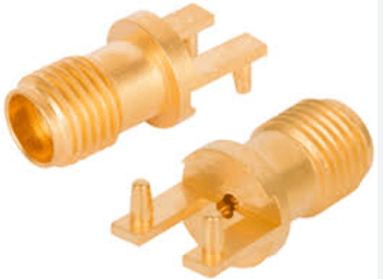
Pcb rf edge connector
Understanding The Basics Of PCB RF Edge Connectors
Printed Circuit Board (PCB) RF edge connectors are integral components in the realm of electronic design, particularly in applications involving radio frequency (RF) signals. These connectors serve as the interface between the PCB and external devices, facilitating the transmission of high-frequency signals with minimal loss. Understanding the basics of PCB RF edge connectors is essential for engineers and designers who aim to optimize the performance of RF circuits.
To begin with, PCB RF edge connectors are designed to connect directly to the edge of a PCB, providing a seamless transition for RF signals.
This design is particularly advantageous in high-frequency applications, as it minimizes the signal path length, thereby reducing potential losses and reflections. The connectors are typically used in applications such as telecommunications, satellite communications, and radar systems, where maintaining signal integrity is paramount.
One of the key considerations in selecting a PCB RF edge connector is the frequency range it can support.
These connectors are engineered to handle specific frequency bands, and choosing the right one is crucial to ensure optimal performance. The frequency range is determined by the connector’s design, including its geometry and the materials used in its construction. For instance, connectors made from high-quality materials such as gold or silver plating can offer superior conductivity and reduced signal loss.
Moreover, the impedance of the connector must match that of the PCB and the connected device to prevent signal reflections.
Most RF applications require a characteristic impedance of 50 ohms, which is a standard in the industry. Mismatched impedance can lead to signal degradation, which is undesirable in high-frequency applications. Therefore, careful consideration of the connector’s impedance is necessary during the design phase.
Another important aspect of PCB RF edge connectors is their mechanical robustness.
These connectors must withstand various environmental conditions, including temperature fluctuations, vibrations, and mechanical stresses. The durability of the connector is often determined by its construction materials and design features, such as locking mechanisms that ensure a secure connection. A reliable connector not only maintains signal integrity but also extends the lifespan of the electronic device.
In addition to mechanical robustness, the ease of installation and maintenance is a significant factor.
PCB RF edge connectors should be designed for straightforward assembly and disassembly, allowing for easy replacement or upgrades. This is particularly important in applications where downtime can be costly, such as in telecommunications infrastructure.
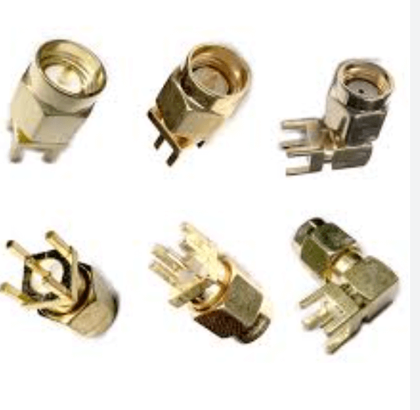
Furthermore, the size and form factor of the connector are critical, especially in compact electronic devices where space is at a premium.
Designers must balance the need for a small footprint with the requirement for high performance. Advances in connector technology have led to the development of miniaturized connectors that do not compromise on performance, making them ideal for modern electronic applications.
In conclusion, PCB RF edge connectors play a vital role in ensuring the efficient transmission of high-frequency signals in various electronic applications. By understanding the fundamental aspects of these connectors, including their frequency range, impedance matching, mechanical robustness, and ease of installation, engineers can make informed decisions that enhance the performance and reliability of their designs. As technology continues to evolve, the demand for high-quality PCB RF edge connectors will undoubtedly grow, underscoring their importance in the field of electronics.
Key Design Considerations For PCB RF Edge Connectors
When designing printed circuit boards (PCBs) for radio frequency (RF) applications, one of the critical components to consider is the RF edge connector. These connectors serve as the interface between the PCB and external devices, ensuring efficient signal transmission and maintaining signal integrity. As RF applications continue to evolve, the demand for high-performance connectors has increased, making it essential to understand the key design considerations for PCB RF edge connectors.
To begin with, impedance matching is a fundamental aspect of RF edge connector design.
Impedance mismatches can lead to signal reflections, which degrade signal quality and reduce the overall performance of the system. Therefore, it is crucial to ensure that the connector’s impedance matches that of the transmission line on the PCB. This can be achieved by carefully selecting the connector’s materials and dimensions, as well as by employing advanced simulation tools to predict and optimize the connector’s performance.
In addition to impedance matching, the frequency range of the application must be taken into account.
RF edge connectors are designed to operate within specific frequency ranges, and selecting a connector that can handle the desired frequency is vital for maintaining signal integrity. As the frequency increases, the potential for signal loss and distortion also rises, necessitating the use of connectors with low insertion loss and high return loss characteristics. These parameters are indicative of the connector’s ability to transmit signals with minimal loss and reflection, respectively.
Moreover, the physical design of the RF edge connector plays a significant role in its performance.
The connector’s geometry, including its size and shape, can impact the electromagnetic fields around it, influencing the signal transmission. Therefore, it is essential to consider the connector’s footprint on the PCB and ensure that it is compatible with the board’s layout. Additionally, the connector’s mechanical robustness is crucial, as it must withstand the physical stresses of insertion and removal without compromising its electrical performance.
Another important consideration is the material selection for the RF edge connector.
The materials used in the connector’s construction can affect its electrical properties, such as conductivity and dielectric constant. High-quality materials, such as gold or silver plating, are often used to enhance conductivity and reduce signal loss. Furthermore, the dielectric materials used in the connector should have low loss tangents to minimize signal attenuation.
Thermal management is also a critical factor in the design of RF edge connectors.
As RF applications often involve high power levels, the connectors can generate significant heat, which can affect their performance and reliability. Effective thermal management strategies, such as the use of heat sinks or thermal vias, can help dissipate heat and maintain the connector’s performance over time.
Finally, manufacturability and cost are practical considerations that cannot be overlooked.
While it is important to prioritize performance, the design of the RF edge connector should also be feasible for mass production and cost-effective. This involves balancing the use of high-performance materials and advanced manufacturing techniques with the need to keep production costs within budget.
In conclusion, designing PCB RF edge connectors requires a comprehensive understanding of various factors, including impedance matching, frequency range, physical design, material selection, thermal management, and manufacturability. By carefully considering these aspects, engineers can develop connectors that meet the demanding requirements of modern RF applications, ensuring reliable and efficient signal transmission.

Advantages Of Using PCB RF Edge Connectors In Modern Electronics
In the rapidly evolving landscape of modern electronics, the demand for efficient and reliable connectivity solutions has never been more critical. Among the myriad of options available, PCB RF edge connectors have emerged as a pivotal component, offering a host of advantages that cater to the intricate needs of contemporary electronic devices. These connectors, designed to facilitate the transmission of radio frequency signals between printed circuit boards (PCBs), are instrumental in ensuring seamless communication and functionality in a wide array of applications.
One of the foremost advantages of using PCB RF edge connectors is their ability to provide high-frequency performance.
As electronic devices become increasingly sophisticated, the need for components that can handle high-speed data transmission without signal degradation is paramount. PCB RF edge connectors are engineered to support high-frequency signals, making them ideal for applications such as telecommunications, aerospace, and advanced computing systems. Their design minimizes signal loss and interference, ensuring that data is transmitted with precision and clarity.
In addition to their high-frequency capabilities, PCB RF edge connectors offer exceptional space-saving benefits.
In an era where miniaturization is a key trend, the compact design of these connectors is particularly advantageous. They allow for efficient use of space on PCBs, enabling manufacturers to design smaller, more lightweight devices without compromising on performance. This is especially beneficial in portable electronics, where space constraints are a significant consideration. By reducing the footprint of the connectors, designers can allocate more space for other critical components, thereby enhancing the overall functionality of the device.
Moreover, PCB RF edge connectors are renowned for their durability and reliability.
Constructed from robust materials, these connectors are designed to withstand harsh environmental conditions, including extreme temperatures and vibrations. This makes them suitable for use in demanding applications such as automotive and industrial electronics, where reliability is non-negotiable. The durability of these connectors ensures a long operational lifespan, reducing the need for frequent replacements and maintenance, which in turn lowers the total cost of ownership for manufacturers and end-users alike.
Another significant advantage of PCB RF edge connectors is their ease of integration. These connectors are designed to be user-friendly, allowing for straightforward installation and removal.
This ease of use is particularly beneficial during the manufacturing process, where time efficiency is crucial. By simplifying the assembly process, PCB RF edge connectors help reduce production time and costs, enabling manufacturers to bring products to market more swiftly. Furthermore, their compatibility with a wide range of PCB designs enhances their versatility, making them a preferred choice for engineers and designers.
In conclusion, the advantages of using PCB RF edge connectors in modern electronics are manifold. Their high-frequency performance, space-saving design, durability, and ease of integration make them an indispensable component in the development of cutting-edge electronic devices. As technology continues to advance, the role of these connectors in facilitating efficient and reliable connectivity will only become more pronounced. By addressing the complex demands of modern electronics, PCB RF edge connectors not only enhance device performance but also contribute to the ongoing innovation and progress within the industry.
Troubleshooting Common Issues With PCB RF Edge Connectors
Printed Circuit Board (PCB) RF edge connectors are critical components in modern electronic systems, facilitating the transmission of radio frequency signals between different parts of a device. However, like any other component, they can encounter issues that may affect the overall performance of the system. Understanding and troubleshooting these common issues is essential for maintaining the integrity and functionality of electronic devices.
One prevalent issue with PCB RF edge connectors is signal loss, which can occur due to several factors.
Poor contact between the connector and the PCB can lead to increased resistance, resulting in signal attenuation. To address this, it is crucial to ensure that the connectors are properly aligned and securely attached to the PCB. Regular inspection and maintenance can help identify any misalignment or wear that may contribute to signal degradation.
Another common problem is impedance mismatch, which can cause signal reflections and standing waves, leading to reduced signal quality.
This issue often arises from improper design or selection of the connector. To mitigate impedance mismatch, it is important to carefully match the impedance of the connector with that of the transmission line. Utilizing simulation tools during the design phase can help predict and correct potential mismatches before they become problematic.
Corrosion and contamination are also significant concerns for PCB RF edge connectors, particularly in environments with high humidity or exposure to corrosive substances.
These factors can lead to increased contact resistance and eventual failure of the connector. To prevent corrosion, it is advisable to use connectors with protective coatings or materials that are resistant to environmental factors. Additionally, implementing regular cleaning protocols can help remove contaminants and prolong the lifespan of the connectors.
Mechanical stress is another factor that can adversely affect the performance of PCB RF edge connectors.
Repeated insertion and removal of connectors can lead to physical wear and damage, compromising the connection. To minimize mechanical stress, it is important to use connectors designed for durability and to handle them with care during installation and maintenance. Employing connectors with robust locking mechanisms can also help maintain a secure connection and reduce the risk of damage.
Thermal issues can also impact the performance of PCB RF edge connectors.
Excessive heat can cause expansion and contraction of materials, leading to mechanical stress and potential failure. To address thermal concerns, it is essential to ensure adequate heat dissipation in the design of the electronic system. This can be achieved through the use of heat sinks, thermal pads, or other cooling solutions. Additionally, selecting connectors made from materials with high thermal stability can help mitigate the effects of temperature fluctuations.
In conclusion, troubleshooting common issues with PCB RF edge connectors requires a comprehensive understanding of the factors that can affect their performance. By addressing signal loss, impedance mismatch, corrosion, mechanical stress, and thermal issues, engineers can ensure the reliability and efficiency of these critical components. Regular maintenance, careful design considerations, and the use of high-quality materials are key strategies in preventing and resolving problems with PCB RF edge connectors. Through these efforts, the integrity of electronic systems can be preserved, ensuring optimal performance in a wide range of applications.