Pcb manufacturing time
Factors Influencing PCB Manufacturing Time
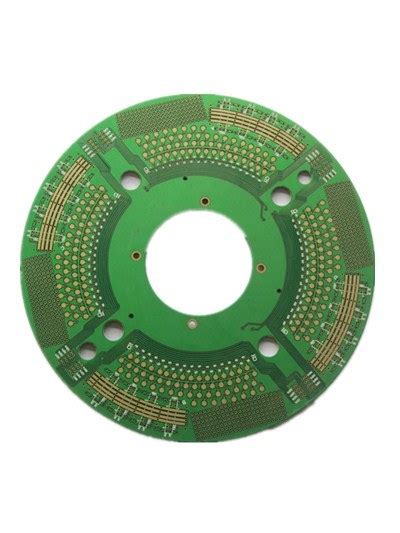
Printed Circuit Board (PCB) manufacturing is a complex process that involves several stages, each contributing to the overall time required to produce a finished product. Understanding the factors influencing PCB manufacturing time is crucial for businesses aiming to optimize production schedules and meet market demands efficiently.
One of the primary factors affecting manufacturing time is the complexity of the PCB design.
As the intricacy of the design increases, so does the time required for manufacturing. Complex designs often involve multiple layers, intricate routing, and a higher number of components, all of which necessitate more detailed planning and execution. Consequently, the design phase, which includes schematic capture and layout, can significantly extend the overall production timeline.
In addition to design complexity, the choice of materials plays a pivotal role in determining manufacturing time.
Different materials have varying properties that can affect the ease and speed of processing. For instance, high-frequency PCBs may require specialized materials that are more challenging to work with, thereby increasing production time. Moreover, the availability of these materials can also impact timelines, as sourcing rare or specialized materials may introduce delays. Transitioning from materials to the manufacturing process itself, the type of technology employed can greatly influence the time required. Traditional manufacturing methods, while reliable, may not be as fast as modern techniques such as automated assembly and surface mount technology (SMT). These advanced methods can significantly reduce production time by streamlining assembly processes and minimizing human intervention.
Furthermore, the scale of production is another critical factor.
Small batch production often allows for quicker turnaround times due to reduced setup and changeover requirements. In contrast, large-scale production may benefit from economies of scale but can be hindered by longer setup times and the need for extensive quality control measures. Therefore, manufacturers must carefully balance production scale with time constraints to achieve optimal results. Quality assurance and testing are indispensable components of PCB manufacturing that also contribute to the overall timeline. Rigorous testing is essential to ensure that the final product meets all specifications and functions correctly. However, this process can be time-consuming, particularly for complex PCBs that require extensive testing procedures. Implementing efficient testing protocols and utilizing automated testing equipment can help mitigate these time demands.
Moreover, the geographical location of the manufacturing facility can influence production time due to logistical considerations.
Facilities located closer to the end market may benefit from reduced shipping times, whereas those situated in regions with well-established supply chains can expedite the procurement of necessary materials and components. Additionally, the regulatory environment in different regions can impact manufacturing timelines, as compliance with local standards and certifications may require additional time and resources. Lastly, the experience and expertise of the manufacturing team are vital in determining the efficiency and speed of the production process. Skilled personnel can identify potential issues early in the design and manufacturing stages, thereby preventing costly and time-consuming rework. Investing in training and retaining experienced staff can thus be a strategic advantage in reducing PCB manufacturing time.
In conclusion, several interrelated factors influence the time required for PCB manufacturing, including design complexity, material selection, manufacturing technology, production scale, quality assurance, geographical location, and team expertise. By understanding and addressing these factors, manufacturers can optimize their processes, reduce lead times, and enhance their competitiveness in the market.
Strategies to Reduce PCB Production Lead Time
In the fast-paced world of electronics, reducing the production lead time for printed circuit boards (PCBs) is crucial for maintaining a competitive edge. As demand for electronic devices continues to grow, manufacturers are under increasing pressure to deliver high-quality products swiftly. To address this challenge, several strategies can be employed to streamline the PCB manufacturing process, thereby minimizing lead times and enhancing overall efficiency.
One effective strategy is to optimize the design phase.
By investing time in thorough design reviews and simulations, potential issues can be identified and rectified before production begins. This proactive approach not only reduces the likelihood of costly errors but also ensures that the design is optimized for manufacturability. Utilizing design for manufacturability (DFM) principles can significantly reduce the time spent on revisions and rework, as it aligns the design with the capabilities and limitations of the manufacturing process.
In addition to design optimization, leveraging advanced technologies can also play a pivotal role in reducing lead times.
Automation, for instance, can expedite various stages of PCB production, from assembly to testing. Automated systems can perform repetitive tasks with precision and speed, thereby freeing up human resources for more complex activities. Moreover, the integration of artificial intelligence and machine learning can enhance decision-making processes, allowing for quicker adjustments and improvements in real-time.
Another critical aspect of reducing PCB production lead time is effective supply chain management.
Establishing strong relationships with reliable suppliers ensures a steady flow of materials, thereby preventing delays caused by shortages or logistical issues. Implementing just-in-time (JIT) inventory practices can further streamline the supply chain by minimizing excess inventory and reducing storage costs. By maintaining close communication with suppliers and utilizing digital tools for tracking and forecasting, manufacturers can anticipate potential disruptions and mitigate their impact on production schedules.
Furthermore, adopting a modular approach to PCB design and production can offer significant time savings.
By standardizing certain components and processes, manufacturers can reduce the complexity and variability of production runs. This not only simplifies assembly but also facilitates quicker transitions between different product lines. Modular designs also allow for easier upgrades and modifications, enabling manufacturers to respond swiftly to changing market demands without extensive redesigns.
Collaboration and communication are also vital in reducing lead times.
Encouraging open lines of communication between design teams, production staff, and suppliers can help identify potential bottlenecks early in the process. Regular meetings and updates ensure that all stakeholders are aligned and informed, allowing for swift resolution of any issues that may arise. Additionally, fostering a culture of continuous improvement encourages employees to identify inefficiencies and propose innovative solutions, further enhancing the speed and quality of production.
Finally, investing in employee training and development is essential for maintaining a skilled workforce capable of adapting to new technologies and processes.
Well-trained employees are more efficient and can contribute to reducing lead times by executing tasks accurately and swiftly. Providing ongoing education and opportunities for skill enhancement not only boosts productivity but also fosters a sense of ownership and commitment among staff.
In conclusion, reducing PCB production lead time requires a multifaceted approach that encompasses design optimization, technological advancements, supply chain management, modular design, effective communication, and employee development. By implementing these strategies, manufacturers can enhance their operational efficiency, meet customer demands more effectively, and maintain a competitive advantage in the ever-evolving electronics industry.
Understanding the PCB Fabrication Process Timeline
Printed Circuit Board (PCB) manufacturing is a complex process that involves several stages, each contributing to the overall timeline of fabrication. Understanding the intricacies of this timeline is crucial for businesses and engineers who rely on timely delivery of PCBs for their projects. The process begins with the design phase, where engineers create detailed schematics and layouts using specialized software. This stage is critical, as any errors in the design can lead to costly delays later in the manufacturing process. Once the design is finalized, it is sent to the manufacturer for the next steps.
The first step in the actual fabrication process is the creation of the PCB substrate, which serves as the foundation for the entire board.
This involves selecting the appropriate materials, such as fiberglass or composite epoxy, and cutting them to the required size. The substrate is then cleaned and prepared for the application of copper layers. This preparation is essential to ensure that the copper adheres properly and that the final product meets the necessary quality standards.
Following the preparation of the substrate, the next stage is the application of the copper layers.
This is typically done through a process called lamination, where thin sheets of copper are bonded to the substrate under heat and pressure. The number of copper layers can vary depending on the complexity of the PCB, with more layers generally leading to longer manufacturing times. Once the copper is applied, the board undergoes a process called etching, where unwanted copper is removed to create the desired circuit patterns. This step requires precision and accuracy, as any mistakes can result in defective boards.
After etching, the PCB goes through a drilling process to create holes for components and vias, which are used to connect different layers of the board.
The drilling must be precise, as even minor deviations can affect the performance of the final product. Once drilling is complete, the holes are plated with copper to ensure electrical connectivity. This plating process can be time-consuming, especially for boards with a high density of holes.
The next stage involves applying a solder mask, which is a protective layer that prevents solder from bridging between conductive traces and causing short circuits.
The solder mask is typically applied using a photolithographic process, which ensures that it is accurately aligned with the underlying copper traces. Following the application of the solder mask, a silkscreen layer is added to the board. This layer contains important information such as component labels and reference designators, which aid in the assembly and testing of the PCB.
Finally, the PCB undergoes a series of inspections and tests to ensure that it meets all specifications and quality standards.
These tests can include electrical testing, visual inspections, and automated optical inspections. Any defects identified during this stage must be addressed before the board can be shipped to the customer. The time required for testing and inspection can vary depending on the complexity of the board and the manufacturer’s quality control processes.
In conclusion, the timeline for PCB manufacturing is influenced by several factors, including the complexity of the design, the number of layers, and the precision required at each stage. By understanding these factors, businesses and engineers can better plan their projects and ensure that they receive their PCBs on time.
Common Delays in PCB Manufacturing and How to Avoid Them
Printed Circuit Board (PCB) manufacturing is a complex process that involves multiple stages, each of which can introduce potential delays. Understanding these common delays and implementing strategies to avoid them is crucial for ensuring timely production and delivery. One of the primary causes of delays in PCB manufacturing is design errors. These errors often arise from inadequate design specifications or oversight during the design phase. To mitigate this, it is essential to conduct thorough design reviews and employ design-for-manufacturability (DFM) checks. By doing so, manufacturers can identify potential issues early in the process, reducing the likelihood of costly and time-consuming revisions later on.
Another significant factor contributing to delays is the procurement of materials.
The availability of specific components can fluctuate due to market demand, leading to extended lead times. To address this, manufacturers should establish strong relationships with reliable suppliers and consider maintaining a buffer stock of critical components. Additionally, early engagement with suppliers during the design phase can help anticipate potential shortages and allow for alternative sourcing strategies. This proactive approach can significantly reduce the risk of material-related delays.
Production bottlenecks also play a role in extending PCB manufacturing time.
These bottlenecks often occur when there is an imbalance in the production line, such as when certain processes take longer than others. To alleviate this issue, manufacturers can implement lean manufacturing principles, which focus on optimizing workflow and eliminating waste. By streamlining production processes and ensuring that each stage is adequately resourced, manufacturers can enhance efficiency and minimize delays.
Quality control is another area where delays can occur.
If a PCB fails to meet quality standards, it may require rework or even complete redesign, both of which can significantly extend production time. To prevent this, manufacturers should implement rigorous quality assurance protocols throughout the production process. This includes regular inspections and testing at various stages of manufacturing to ensure that any defects are identified and addressed promptly. By maintaining high-quality standards, manufacturers can reduce the likelihood of rework and associated delays.
Communication breakdowns between different teams involved in the PCB manufacturing process can also lead to delays.
Misunderstandings or lack of information can result in errors or misaligned expectations, which can slow down production. To avoid this, it is crucial to establish clear communication channels and ensure that all stakeholders are kept informed throughout the process. Regular meetings and updates can help align teams and facilitate the smooth flow of information, thereby reducing the potential for delays.
Finally, unforeseen technical issues can arise during the manufacturing process, causing unexpected delays.
While it is impossible to predict every potential problem, manufacturers can prepare by investing in robust contingency plans and maintaining a flexible production schedule. This allows for quick adjustments in response to technical challenges, minimizing their impact on overall production time.
In conclusion, while delays in PCB manufacturing are common, they can often be avoided through careful planning and proactive management. By addressing design errors, ensuring timely procurement of materials, optimizing production processes, maintaining high-quality standards, fostering effective communication, and preparing for technical challenges, manufacturers can significantly reduce the likelihood of delays. These strategies not only enhance efficiency but also contribute to the timely delivery of high-quality PCBs, ultimately benefiting both manufacturers and their clients.