High frequency pcb signal
Understanding High Frequency PCB Signal Integrity
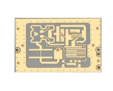
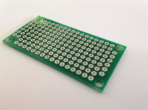
In the realm of modern electronics, the demand for high-speed communication and processing has led to the proliferation of high frequency printed circuit boards (PCBs). These PCBs are integral to the performance of a wide array of devices, from telecommunications equipment to advanced computing systems.
Understanding the intricacies of high frequency PCB signal integrity is crucial for engineers and designers aiming to optimize the performance and reliability of these systems. Signal integrity, in this context, refers to the ability of a signal to propagate through a PCB without distortion or loss of quality. As frequencies increase, maintaining signal integrity becomes increasingly challenging due to a variety of factors.
One of the primary challenges in high frequency PCB design is the management of electromagnetic interference (EMI).
At high frequencies, signals can easily couple with adjacent traces or components, leading to crosstalk and signal degradation. To mitigate these effects, designers often employ techniques such as controlled impedance routing and the use of ground planes. Controlled impedance ensures that the characteristic impedance of a trace matches the source and load, minimizing reflections and signal loss. Ground planes, on the other hand, provide a return path for signals and help shield sensitive traces from external interference.
Moreover, the choice of materials plays a pivotal role in high frequency PCB design.
Traditional FR-4 substrates, commonly used in low-frequency applications, may not be suitable for high frequency circuits due to their higher dielectric losses. Instead, materials with lower dielectric constants and loss tangents, such as Rogers or Teflon-based laminates, are preferred. These materials help reduce signal attenuation and maintain signal integrity over longer distances. Additionally, the thickness and width of traces must be carefully calculated to ensure they can handle the desired frequency without excessive loss or distortion.
Another critical aspect of high frequency PCB signal integrity is the management of signal reflections
Reflections occur when there is a mismatch in impedance along the transmission path, causing a portion of the signal to be reflected back towards the source. This can lead to signal distortion and timing issues, particularly in high-speed digital circuits. To address this, designers often use termination techniques, such as series or parallel resistors, to match the impedance at the end of a transmission line, thereby minimizing reflections.
Furthermore, the layout of components on a high frequency PCB can significantly impact signal integrity.
Components should be placed to minimize the length of high-speed traces and reduce the potential for EMI. Additionally, careful attention must be paid to the routing of differential pairs, which are commonly used in high-speed applications to reduce noise and improve signal integrity. Differential pairs should be routed with consistent spacing and length to ensure that the signals remain synchronized and immune to common-mode noise.
In conclusion, maintaining signal integrity in high frequency PCBs is a complex task that requires careful consideration of various factors, including EMI management, material selection, impedance control, and component layout. By understanding and addressing these challenges, engineers can design PCBs that meet the demanding requirements of modern high-speed applications. As technology continues to advance, the importance of mastering high frequency PCB signal integrity will only grow, underscoring the need for ongoing research and innovation in this critical field.

Design Techniques for High Frequency PCB Signals
Designing printed circuit boards (PCBs) for high-frequency signals presents unique challenges that require careful consideration and precise techniques to ensure optimal performance. As electronic devices continue to evolve, the demand for high-speed data transmission and increased functionality has led to the proliferation of high-frequency applications. Consequently, engineers must employ specialized design techniques to mitigate issues such as signal integrity, electromagnetic interference, and thermal management.
To begin with, understanding the fundamental principles of high-frequency signal behavior is crucial.
At high frequencies, signals tend to behave more like electromagnetic waves rather than simple electrical currents. This shift necessitates a focus on impedance control, as mismatched impedance can lead to signal reflections, which degrade signal integrity. Therefore, maintaining consistent impedance throughout the PCB traces is essential. This can be achieved by carefully selecting the trace width, spacing, and the dielectric material of the PCB substrate. Utilizing controlled impedance traces ensures that the signal maintains its integrity as it travels across the board.
Moreover, the layout of the PCB plays a pivotal role in high-frequency design.
Minimizing the length of signal paths is a fundamental strategy, as longer paths can introduce unwanted inductance and capacitance, which can distort the signal. Additionally, the use of ground planes is a common practice to provide a return path for signals, thereby reducing electromagnetic interference and crosstalk between adjacent traces. Ground planes also help in maintaining a uniform impedance, further enhancing signal integrity.
Transitioning to the topic of materials, the choice of substrate material is another critical factor in high-frequency PCB design.
Traditional FR-4 material, commonly used in low-frequency applications, may not be suitable for high-frequency signals due to its higher dielectric loss. Instead, materials such as Rogers or Teflon, which offer lower dielectric constants and loss tangents, are preferred. These materials help in reducing signal attenuation and maintaining signal speed, which is vital for high-frequency applications.
In addition to material selection, the use of vias in high-frequency PCBs requires careful consideration.
Vias, which are used to connect different layers of a PCB, can introduce parasitic inductance and capacitance, potentially affecting signal performance. To mitigate these effects, it is advisable to minimize the number of vias used in high-frequency signal paths. When vias are necessary, techniques such as back-drilling can be employed to remove the unused portion of the via, thereby reducing its parasitic effects.
Furthermore, thermal management is an often-overlooked aspect of high-frequency PCB design.
High-frequency components can generate significant heat, which, if not properly managed, can lead to performance degradation or failure. Implementing adequate thermal vias, heat sinks, and thermal pads can help dissipate heat effectively, ensuring the reliability and longevity of the PCB.
In conclusion, designing PCBs for high-frequency signals demands a comprehensive understanding of electromagnetic principles and meticulous attention to detail. By focusing on impedance control, optimizing layout, selecting appropriate materials, managing vias, and addressing thermal concerns, engineers can create high-frequency PCBs that meet the stringent requirements of modern electronic applications. As technology continues to advance, the importance of these design techniques will only grow, underscoring the need for ongoing innovation and expertise in the field of high-frequency PCB design.
Material Selection for High Frequency PCB Signal Performance
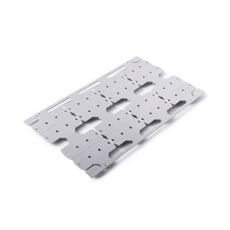
In the realm of high-frequency printed circuit boards (PCBs), the selection of materials plays a pivotal role in determining signal performance. As electronic devices continue to evolve, demanding faster speeds and higher frequencies, the importance of choosing the right materials becomes increasingly critical. High-frequency PCBs are utilized in a variety of applications, including telecommunications, aerospace, and advanced computing, where signal integrity and performance are paramount. Therefore, understanding the factors that influence material selection is essential for engineers and designers aiming to optimize high-frequency PCB signal performance.
To begin with, dielectric constant (Dk) is a fundamental property that significantly impacts signal speed and integrity.
Materials with a low and stable dielectric constant are preferred for high-frequency applications because they facilitate faster signal propagation and reduce signal loss. Consistency in Dk across a range of frequencies ensures that the signal remains stable, minimizing distortion and maintaining integrity. Consequently, materials such as PTFE (polytetrafluoroethylene) and certain ceramic-filled laminates are often chosen for their favorable dielectric properties.
In addition to dielectric constant, the dissipation factor (Df) is another critical parameter to consider.
The dissipation factor measures the inherent energy loss of a material as it conducts an alternating current. A lower dissipation factor indicates that the material is more efficient at transmitting signals with minimal loss, which is crucial for maintaining signal strength and clarity at high frequencies. Materials with low Df values, such as Rogers laminates, are frequently selected for high-frequency PCBs to ensure optimal performance.
Moreover, thermal management is a key consideration in material selection for high-frequency PCBs.
As frequencies increase, so does the potential for heat generation, which can adversely affect signal performance and the overall reliability of the PCB. Therefore, materials with good thermal conductivity are essential to dissipate heat effectively and maintain the stability of the circuit. High-frequency PCB materials often incorporate fillers or are designed with specific structures to enhance thermal management capabilities.
Furthermore, the coefficient of thermal expansion (CTE) is an important factor that influences material selection.
A material’s CTE describes how it expands or contracts with temperature changes. In high-frequency applications, mismatched CTE between the PCB material and other components can lead to mechanical stress and potential failure. Selecting materials with a CTE that closely matches that of the components ensures mechanical stability and longevity of the PCB.
Additionally, surface finish and copper roughness are aspects that cannot be overlooked.
The surface finish affects the skin effect, where high-frequency signals tend to travel on the surface of conductors. A smoother surface finish reduces signal loss and improves performance. Similarly, copper roughness can impact signal integrity; therefore, materials with smoother copper surfaces are preferred to minimize signal attenuation.
In conclusion, the selection of materials for high-frequency PCBs is a complex process that requires careful consideration of various factors, including dielectric constant, dissipation factor, thermal management, coefficient of thermal expansion, and surface characteristics. By understanding and prioritizing these properties, engineers and designers can ensure that their high-frequency PCBs deliver optimal signal performance, meeting the demands of modern electronic applications. As technology continues to advance, the importance of meticulous material selection will only grow, underscoring its critical role in the development of high-performance electronic systems.
Challenges in High Frequency PCB Signal Routing
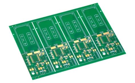
In the realm of modern electronics, high frequency printed circuit boards (PCBs) have become indispensable, particularly in applications such as telecommunications, radar systems, and advanced computing. However, the routing of signals on these high frequency PCBs presents a unique set of challenges that engineers must navigate to ensure optimal performance and reliability. As frequencies increase, the behavior of electrical signals becomes more complex, necessitating a deeper understanding of electromagnetic theory and meticulous attention to design details.
One of the primary challenges in high frequency PCB signal routing is managing signal integrity.
At high frequencies, signals are more susceptible to distortion and loss, which can degrade the performance of the entire system. This is largely due to the skin effect, where the effective resistance of a conductor increases with frequency, causing signal attenuation. To mitigate this, designers often use materials with lower dielectric losses and employ techniques such as impedance matching to minimize reflections and ensure that signals are transmitted efficiently across the board.
Moreover, crosstalk between adjacent traces is another significant concern.
As signal frequencies rise, the electromagnetic fields associated with these signals can couple more easily between nearby traces, leading to unwanted interference. This can be particularly problematic in densely packed PCBs where space constraints limit the distance between traces. To address this, engineers may use differential signaling, which involves routing pairs of traces together to cancel out noise, or they may implement shielding techniques to isolate sensitive signals from potential sources of interference.
In addition to signal integrity and crosstalk, thermal management becomes increasingly critical in high frequency applications.
The increased power consumption associated with high frequency operation can lead to significant heat generation, which, if not properly managed, can affect the performance and longevity of the PCB. Effective thermal management strategies, such as the use of thermal vias, heat sinks, and advanced materials with high thermal conductivity, are essential to dissipate heat and maintain the reliability of the system.
Furthermore, the choice of substrate material plays a crucial role in high frequency PCB design.
Traditional FR-4 substrates, commonly used in lower frequency applications, may not provide the necessary performance at higher frequencies due to their higher dielectric losses. Instead, materials such as PTFE (polytetrafluoroethylene) or ceramics, which offer lower dielectric constants and better thermal stability, are often preferred. However, these materials can be more expensive and challenging to work with, requiring specialized manufacturing processes.
Transitioning from design to manufacturing, the precision of fabrication processes is paramount.
High frequency PCBs demand tighter tolerances and more accurate etching to ensure that the physical dimensions of traces and other features align with the design specifications. Any deviation can lead to impedance mismatches and other issues that compromise signal integrity. Therefore, collaboration between design and manufacturing teams is essential to achieve the desired performance outcomes.
In conclusion, while high frequency PCB signal routing presents a myriad of challenges, advancements in materials, design techniques, and manufacturing processes continue to push the boundaries of what is possible. By addressing issues related to signal integrity, crosstalk, thermal management, and material selection, engineers can develop high frequency PCBs that meet the demanding requirements of modern electronic applications. As technology continues to evolve, ongoing research and innovation will be crucial in overcoming these challenges and unlocking new possibilities in high frequency electronics.

