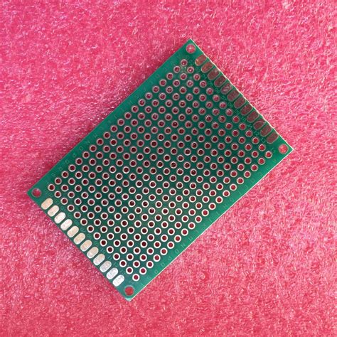
Heavy copper pcb design
Advantages Of Heavy Copper PCB In Power Electronics
In the realm of power electronics, the design and implementation of printed circuit boards (PCBs) play a crucial role in determining the efficiency and reliability of electronic devices. Among the various types of PCBs, heavy copper PCBs have emerged as a significant innovation, offering numerous advantages that cater specifically to the demands of power electronics. As the name suggests, heavy copper PCBs are characterized by their thick copper layers, which typically exceed three ounces per square foot. This distinctive feature endows them with several benefits that are particularly advantageous in power electronics applications.
To begin with, one of the primary advantages of heavy copper PCBs is their enhanced current-carrying capacity.
The increased thickness of the copper layers allows these PCBs to handle higher currents without overheating, which is a critical requirement in power electronics. This capability not only ensures the efficient operation of high-power devices but also contributes to their longevity by minimizing the risk of thermal damage. Consequently, heavy copper PCBs are often employed in applications such as power converters, power supplies, and motor controllers, where high current levels are prevalent.
Moreover, heavy copper PCBs exhibit superior thermal management properties.
The thick copper layers facilitate effective heat dissipation, which is essential for maintaining optimal operating temperatures in power electronic devices. By efficiently spreading and dissipating heat, these PCBs help prevent hotspots and thermal stress, thereby enhancing the overall reliability and performance of the electronic system. This attribute is particularly beneficial in applications where thermal management is a critical concern, such as in automotive electronics and industrial power systems.
In addition to their thermal advantages, heavy copper PCBs also offer improved mechanical strength.
The robust construction of these PCBs makes them more resistant to mechanical stresses, such as bending and vibration, which are common in demanding environments. This increased durability ensures that the PCBs can withstand harsh operating conditions, making them suitable for use in rugged applications like aerospace and military electronics.
Furthermore, heavy copper PCBs enable the integration of complex circuitry on a single board.
The thick copper layers allow for the incorporation of multiple layers and intricate designs, which can accommodate a wide range of components and functionalities. This capability not only simplifies the design process but also reduces the overall size and weight of the electronic system, which is a significant advantage in applications where space and weight are at a premium.
Another noteworthy benefit of heavy copper PCBs is their ability to support high-density interconnections.
The thick copper layers provide ample surface area for creating reliable and robust connections between components, which is essential for ensuring signal integrity and minimizing electrical losses. This feature is particularly advantageous in high-frequency applications, where maintaining signal quality is paramount.
In conclusion, heavy copper PCBs offer a multitude of advantages that make them an ideal choice for power electronics applications. Their enhanced current-carrying capacity, superior thermal management, improved mechanical strength, and ability to support complex circuitry and high-density interconnections collectively contribute to the efficiency, reliability, and performance of electronic devices. As the demand for high-power and high-performance electronic systems continues to grow, the adoption of heavy copper PCBs is likely to become increasingly prevalent, underscoring their significance in the field of power electronics.
Design Considerations For Heavy Copper PCBs
In the realm of printed circuit board (PCB) design, heavy copper PCBs have emerged as a critical solution for applications requiring high current or enhanced thermal management. These PCBs are characterized by their use of copper weights exceeding three ounces per square foot, which significantly enhances their ability to conduct electricity and dissipate heat. As such, they are particularly valuable in industries such as power electronics, automotive, and renewable energy, where reliability and performance are paramount. However, designing heavy copper PCBs involves a unique set of considerations that must be meticulously addressed to ensure optimal functionality and longevity.
To begin with, one of the primary considerations in heavy copper PCB design is the selection of appropriate materials.
The choice of substrate material is crucial, as it must be able to withstand the increased thermal and mechanical stresses associated with heavy copper layers. Typically, high-temperature laminates are preferred, as they offer superior thermal stability and mechanical strength. Additionally, the dielectric material must be carefully chosen to ensure it can handle the increased thermal conductivity without degrading over time.
Moreover, the design of the trace layout is another critical aspect that requires careful attention.
With heavy copper PCBs, the trace width and spacing must be meticulously calculated to accommodate the higher current loads. This often involves using wider traces and larger pads to reduce the risk of overheating and to ensure efficient current distribution. Furthermore, the use of thermal reliefs and vias is essential to facilitate heat dissipation and to prevent localized hotspots, which can lead to premature failure of the PCB.
Transitioning to the manufacturing process, it is important to note that heavy copper PCBs require specialized fabrication techniques.
The increased copper thickness necessitates the use of advanced etching and plating processes to achieve the desired trace geometries and layer configurations. This often involves multiple plating cycles and the use of specialized etching solutions to ensure precise control over the copper deposition. Consequently, collaboration with experienced manufacturers who possess the necessary expertise and equipment is vital to achieving high-quality results.
In addition to the technical aspects, cost considerations also play a significant role in the design of heavy copper PCBs.
The use of thicker copper layers and specialized materials inevitably leads to higher production costs. Therefore, it is essential to conduct a thorough cost-benefit analysis to determine the most cost-effective design that meets the performance requirements. This may involve optimizing the layer stack-up, minimizing the number of layers, or exploring alternative materials that offer a balance between performance and cost.
Finally, testing and validation are indispensable components of the heavy copper PCB design process.
Given the critical applications in which these PCBs are used, rigorous testing is necessary to ensure they meet the required electrical, thermal, and mechanical specifications. This includes conducting thermal cycling tests, electrical load tests, and mechanical stress tests to verify the PCB’s reliability under real-world conditions.
In conclusion, the design of heavy copper PCBs is a complex process that demands careful consideration of material selection, trace layout, manufacturing techniques, cost implications, and testing protocols. By addressing these factors with precision and expertise, designers can create robust and reliable PCBs that meet the demanding requirements of high-performance applications. As technology continues to advance, the importance of heavy copper PCBs is likely to grow, underscoring the need for continued innovation and excellence in their design and manufacturing.
Thermal Management Techniques In Heavy Copper PCB Design
In the realm of electronics, the design of printed circuit boards (PCBs) plays a crucial role in ensuring the efficient operation of devices. Among the various types of PCBs, heavy copper PCBs are particularly noteworthy due to their ability to handle high current loads and dissipate heat effectively. As electronic devices become more powerful and compact, the need for effective thermal management techniques in heavy copper PCB design becomes increasingly important. This article explores the various strategies employed to manage heat in these robust PCBs, ensuring optimal performance and longevity.
To begin with, heavy copper PCBs are characterized by their thick copper layers, typically ranging from 3 ounces per square foot to over 20 ounces.
This increased copper thickness allows for higher current carrying capacity and improved thermal conductivity. However, the challenge lies in managing the heat generated by these high currents. One fundamental technique involves the use of thermal vias, which are small holes filled or plated with copper that connect the different layers of the PCB. These vias facilitate the transfer of heat from the surface of the board to the inner layers or to a heat sink, thereby preventing localized overheating.
In addition to thermal vias, the layout of the PCB itself plays a significant role in thermal management.
By strategically placing components and copper traces, designers can optimize the flow of heat across the board. For instance, high-power components should be positioned in such a way that heat is evenly distributed, minimizing hotspots. Moreover, the use of wider traces and larger pads can further enhance heat dissipation, as they provide a greater surface area for heat to spread.
Another effective technique is the incorporation of thermal reliefs, which are small gaps in the copper pour around a pad.
These gaps reduce the amount of heat conducted to the pad, thereby preventing soldering issues during assembly. While thermal reliefs are primarily used to aid in the soldering process, they also contribute to the overall thermal management strategy by controlling the heat flow within the PCB.
Furthermore, the choice of materials in heavy copper PCB design is critical for effective thermal management.
High thermal conductivity substrates, such as aluminum or ceramic, can be used to enhance heat dissipation. These materials act as a heat spreader, distributing heat more evenly across the board and reducing the risk of thermal stress. Additionally, the use of thermal interface materials (TIMs) between the PCB and heat sinks can further improve heat transfer efficiency.
Moreover, advanced simulation tools have become indispensable in the design process, allowing engineers to model and predict the thermal behavior of heavy copper PCBs.
By simulating different scenarios, designers can identify potential thermal issues and optimize the PCB layout before physical prototyping. This not only saves time and resources but also ensures that the final product meets the desired thermal performance criteria.
In conclusion, the design of heavy copper PCBs necessitates a comprehensive approach to thermal management. By employing techniques such as thermal vias, strategic component placement, thermal reliefs, and the use of high-conductivity materials, designers can effectively manage heat and enhance the performance and reliability of electronic devices. As technology continues to advance, the importance of these thermal management strategies will only grow, underscoring the need for continued innovation in heavy copper PCB design.
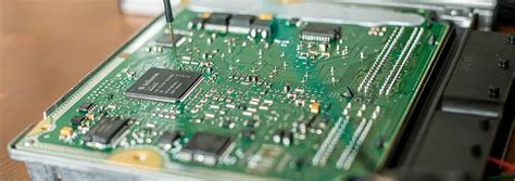
Applications Of Heavy Copper PCBs In Industrial Sectors
Heavy copper PCBs, characterized by their thick copper layers, have become increasingly significant in various industrial sectors due to their enhanced durability and superior thermal management capabilities. These printed circuit boards, which typically feature copper thicknesses ranging from 3 oz/ft² to over 20 oz/ft², are engineered to withstand high current loads and extreme environmental conditions. As industries continue to demand more robust and reliable electronic components, the applications of heavy copper PCBs have expanded, offering solutions that meet the rigorous requirements of modern industrial operations.
One of the primary applications of heavy copper PCBs is in the power electronics sector.
These PCBs are integral to the design and manufacture of power supplies, inverters, and converters, where they facilitate efficient power distribution and management. The ability of heavy copper PCBs to handle high current levels without overheating makes them ideal for these applications. Moreover, their enhanced thermal conductivity ensures that heat is dissipated effectively, thereby prolonging the lifespan of the components and improving overall system reliability. This is particularly crucial in industries such as renewable energy, where power electronics play a pivotal role in the conversion and distribution of energy from sources like solar panels and wind turbines.
In addition to power electronics, heavy copper PCBs are extensively used in the automotive industry.
As vehicles become more technologically advanced, the demand for reliable electronic systems has surged. Heavy copper PCBs are employed in various automotive applications, including electric vehicle charging systems, power steering, and braking systems. Their ability to withstand high temperatures and mechanical stress makes them suitable for the harsh conditions often encountered in automotive environments. Furthermore, the growing trend towards electric and hybrid vehicles has further amplified the need for heavy copper PCBs, as these vehicles require efficient power management systems to operate effectively.
The telecommunications industry also benefits from the use of heavy copper PCBs.
With the ever-increasing demand for faster and more reliable communication networks, the infrastructure supporting these networks must be robust and efficient. Heavy copper PCBs are used in the construction of base stations, routers, and other critical communication equipment. Their superior electrical conductivity and thermal management capabilities ensure that these devices can handle high data loads and operate continuously without failure. This reliability is essential in maintaining seamless communication services, which are vital for both personal and business operations.
Moreover, heavy copper PCBs find applications in the aerospace and defense sectors, where reliability and performance are of utmost importance.
In these industries, electronic components are often exposed to extreme conditions, including high altitudes, temperature fluctuations, and mechanical vibrations. Heavy copper PCBs are used in avionics, radar systems, and other critical defense equipment, where their robustness and ability to manage high power loads are indispensable. The use of these PCBs ensures that aerospace and defense systems remain operational and effective, even in the most challenging environments.
In conclusion, the applications of heavy copper PCBs in industrial sectors are diverse and continue to grow as technology advances. Their unique properties, including high current carrying capacity, excellent thermal management, and durability, make them indispensable in power electronics, automotive, telecommunications, aerospace, and defense industries. As these sectors evolve and demand more reliable and efficient electronic components, heavy copper PCBs will undoubtedly play a crucial role in meeting these needs, driving innovation and enhancing performance across various industrial applications.