High frequency pcb manufacture
Innovations In High Frequency PCB Manufacturing Techniques
In recent years, the field of high frequency printed circuit board (PCB) manufacturing has witnessed significant advancements, driven by the increasing demand for faster and more efficient electronic devices. As technology continues to evolve, manufacturers are compelled to innovate and refine their techniques to meet the stringent requirements of high frequency applications. These innovations are not only enhancing the performance of electronic devices but also paving the way for new possibilities in various industries.
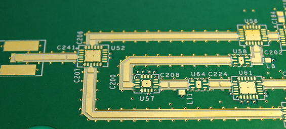
One of the key innovations in high frequency PCB manufacturing is the development of advanced materials.
Traditional materials, such as FR-4, are often inadequate for high frequency applications due to their dielectric properties. Consequently, manufacturers are turning to specialized materials like PTFE (polytetrafluoroethylene) and ceramic-filled laminates, which offer superior electrical performance and thermal stability. These materials minimize signal loss and ensure that the PCBs can handle the high-speed data transmission required in modern applications.
In addition to material advancements, precision in manufacturing processes has become paramount.
The miniaturization of electronic components necessitates tighter tolerances and more accurate fabrication techniques. To address this, manufacturers are employing state-of-the-art equipment, such as laser direct imaging (LDI) systems, which allow for precise patterning of circuit traces. This technology not only improves the accuracy of the PCB layout but also reduces the time required for prototyping and production, thereby accelerating the development cycle.
Moreover, the integration of automated processes in PCB manufacturing has revolutionized the industry.
Automation enhances consistency and reduces human error, which is crucial for maintaining the high quality standards required in high frequency applications. Automated optical inspection (AOI) systems, for instance, are now widely used to detect defects in PCBs at various stages of production. This ensures that any issues are identified and rectified early, preventing costly rework and ensuring that the final product meets the desired specifications.
Furthermore, the rise of computer-aided design (CAD) software has significantly impacted the design and manufacturing of high frequency PCBs.
These sophisticated tools enable engineers to simulate and optimize PCB designs before they are physically produced. By using CAD software, manufacturers can predict how a PCB will perform under different conditions, allowing for adjustments to be made in the design phase. This not only improves the reliability of the final product but also reduces the likelihood of costly design iterations.
Another noteworthy innovation is the adoption of advanced surface finish techniques.
High frequency PCBs often require specific surface finishes to ensure optimal signal integrity and performance. Techniques such as electroless nickel immersion gold (ENIG) and immersion silver are increasingly being used to provide a smooth and conductive surface, which is essential for high frequency applications. These finishes also offer excellent corrosion resistance, thereby extending the lifespan of the PCBs.
In conclusion, the innovations in high frequency PCB manufacturing techniques are transforming the landscape of electronic device production. Through the development of advanced materials, precision manufacturing processes, automation, CAD software, and surface finish techniques, manufacturers are able to meet the growing demands of high frequency applications. As technology continues to advance, it is likely that further innovations will emerge, driving the industry towards even greater levels of performance and efficiency. These advancements not only benefit manufacturers but also have far-reaching implications for various sectors, including telecommunications, aerospace, and consumer electronics, where high frequency PCBs play a critical role.
Key Challenges Faced By High Frequency PCB Manufacturers
High frequency printed circuit boards (PCBs) are integral components in the rapidly evolving landscape of modern electronics, particularly in applications such as telecommunications, aerospace, and advanced computing. As the demand for high-speed and high-performance electronic devices continues to grow, manufacturers of high frequency PCBs face a myriad of challenges that require innovative solutions and meticulous attention to detail.
One of the primary challenges is the selection of suitable materials.
High frequency PCBs require substrates with low dielectric constants and minimal loss tangents to ensure signal integrity and minimize signal loss. However, these materials can be expensive and difficult to source, posing a significant challenge for manufacturers striving to balance performance with cost-effectiveness.
In addition to material selection, the design and fabrication processes of high frequency PCBs present their own set of challenges.
The intricate designs necessary for high frequency applications demand precision and accuracy, as even the slightest deviation can lead to performance degradation. Manufacturers must employ advanced design software and state-of-the-art fabrication techniques to ensure that the PCBs meet the stringent requirements of high frequency applications. Moreover, the miniaturization trend in electronics further complicates the design process, as manufacturers must pack more functionality into smaller spaces without compromising performance.
Thermal management is another critical challenge faced by high frequency PCB manufacturers.
As electronic devices operate at higher frequencies, they generate more heat, which can adversely affect performance and reliability. Effective thermal management solutions are essential to dissipate heat and maintain optimal operating conditions. Manufacturers must carefully consider the thermal properties of materials and incorporate innovative cooling solutions, such as heat sinks and thermal vias, to address this challenge.
Furthermore, the testing and quality assurance of high frequency PCBs are complex and demanding processes.
Ensuring that these PCBs meet the required performance standards necessitates rigorous testing procedures, which can be time-consuming and costly. Manufacturers must invest in advanced testing equipment and develop comprehensive testing protocols to identify and rectify any defects or performance issues. This is particularly important given the high stakes involved in applications such as aerospace and telecommunications, where failure is not an option.
Supply chain management also poses a significant challenge for high frequency PCB manufacturers.
The global nature of the electronics industry means that manufacturers must navigate complex supply chains to source the necessary materials and components. Disruptions in the supply chain, whether due to geopolitical tensions, natural disasters, or other unforeseen events, can lead to delays and increased costs. Manufacturers must develop robust supply chain strategies and establish strong relationships with suppliers to mitigate these risks.
Finally, the rapid pace of technological advancement presents an ongoing challenge for high frequency PCB manufacturers.
As new technologies emerge and industry standards evolve, manufacturers must continuously adapt and innovate to remain competitive. This requires ongoing investment in research and development, as well as a commitment to staying abreast of the latest industry trends and advancements.
In conclusion, high frequency PCB manufacturers face a range of challenges that require a combination of technical expertise, strategic planning, and innovative thinking. From material selection and design intricacies to thermal management and supply chain complexities, these challenges underscore the importance of adaptability and resilience in the ever-changing landscape of high frequency electronics. By addressing these challenges head-on, manufacturers can continue to deliver high-performance PCBs that meet the demands of modern technology.
The Role Of Material Selection In High Frequency PCB Production
In the realm of high frequency printed circuit board (PCB) production, the selection of materials plays a pivotal role in determining the performance, reliability, and efficiency of the final product. As electronic devices continue to evolve, demanding faster speeds and higher frequencies, the importance of choosing the right materials becomes increasingly critical. High frequency PCBs are utilized in a variety of applications, including telecommunications, aerospace, and advanced computing, where signal integrity and minimal loss are paramount. Therefore, understanding the nuances of material selection is essential for manufacturers aiming to meet the stringent requirements of these advanced applications.
To begin with, the dielectric material used in high frequency PCBs is a fundamental consideration.
Dielectric materials are responsible for insulating the conductive layers and maintaining signal integrity. The dielectric constant (Dk) and dissipation factor (Df) of these materials are crucial parameters that influence the performance of high frequency circuits. A low dielectric constant is preferred as it allows for faster signal propagation, while a low dissipation factor minimizes signal loss. Materials such as PTFE (polytetrafluoroethylene), ceramic-filled laminates, and hydrocarbon-based laminates are commonly used due to their favorable electrical properties. These materials offer a balance between performance and manufacturability, making them suitable for high frequency applications.
Moreover, thermal management is another critical aspect influenced by material selection.
High frequency PCBs often operate in environments where heat dissipation is a concern. Therefore, materials with good thermal conductivity are essential to prevent overheating and ensure the longevity of the PCB. Copper, known for its excellent thermal and electrical conductivity, is typically used for the conductive layers. However, the choice of substrate material also impacts thermal performance. For instance, ceramic-filled laminates not only provide low dielectric loss but also offer superior thermal management capabilities compared to traditional FR-4 materials.
In addition to electrical and thermal considerations, mechanical properties of the materials cannot be overlooked.
High frequency PCBs must withstand various environmental stresses, including vibration, mechanical shock, and temperature fluctuations. Therefore, materials with robust mechanical properties are necessary to ensure the structural integrity of the PCB. PTFE-based materials, while offering excellent electrical properties, can be mechanically challenging to work with due to their flexibility. Manufacturers often reinforce these materials with glass fibers to enhance their mechanical strength without compromising their electrical performance.
Furthermore, the manufacturing process itself is influenced by the choice of materials.
Some high performance materials may require specialized fabrication techniques, which can impact production costs and lead times. For instance, PTFE materials often necessitate specific drilling and plating processes due to their unique properties. Consequently, manufacturers must carefully consider the trade-offs between material performance and manufacturability to optimize production efficiency.
In conclusion, the role of material selection in high frequency PCB production is multifaceted, encompassing electrical, thermal, mechanical, and manufacturing considerations. As the demand for high frequency applications continues to grow, manufacturers must remain vigilant in selecting materials that not only meet the technical requirements but also align with production capabilities. By doing so, they can ensure the development of high frequency PCBs that deliver optimal performance and reliability in their intended applications. Through careful material selection, manufacturers can address the challenges posed by high frequency environments and contribute to the advancement of modern electronic technologies.

Future Trends In High Frequency PCB Manufacturing Technology
The landscape of high frequency PCB (Printed Circuit Board) manufacturing is undergoing significant transformation, driven by rapid technological advancements and evolving market demands. As industries such as telecommunications, automotive, and consumer electronics continue to push the boundaries of innovation, the need for high frequency PCBs that can support faster data transmission and higher performance is becoming increasingly critical. Consequently, manufacturers are exploring new technologies and methodologies to meet these demands, setting the stage for future trends in this dynamic field.
One of the most prominent trends in high frequency PCB manufacturing is the integration of advanced materials.
Traditional materials like FR-4 are gradually being supplemented or replaced by high-performance substrates such as PTFE (Polytetrafluoroethylene) and ceramic-filled laminates. These materials offer superior dielectric properties and thermal stability, which are essential for maintaining signal integrity at high frequencies. As the demand for higher data rates and reduced signal loss continues to grow, the adoption of these advanced materials is expected to become more widespread.
In addition to material innovation, the miniaturization of components is another trend shaping the future of high frequency PCB manufacturing.
As electronic devices become more compact, the need for smaller, more efficient PCBs is paramount. Manufacturers are increasingly employing techniques such as microvia technology and high-density interconnects (HDI) to achieve greater component density and improved electrical performance. This trend not only supports the development of smaller devices but also enhances the overall functionality and reliability of high frequency PCBs.
Moreover, the rise of 5G technology is acting as a catalyst for advancements in high frequency PCB manufacturing.
The deployment of 5G networks requires PCBs that can operate at millimeter-wave frequencies, necessitating precise manufacturing processes and stringent quality control measures. To address these challenges, manufacturers are investing in state-of-the-art equipment and adopting automated production techniques. Automation not only improves manufacturing efficiency but also ensures consistent quality, which is crucial for meeting the rigorous standards of 5G applications.
Furthermore, the increasing complexity of electronic systems is driving the need for more sophisticated design and simulation tools.
High frequency PCB manufacturers are leveraging advanced software solutions to optimize the design process, enabling them to predict and mitigate potential issues before they arise. These tools facilitate the creation of more intricate PCB layouts, allowing for better signal routing and reduced electromagnetic interference. As a result, manufacturers can deliver high-performance PCBs that meet the specific requirements of their clients.
Sustainability is also emerging as a key consideration in the future of high frequency PCB manufacturing.
As environmental concerns gain prominence, manufacturers are exploring eco-friendly materials and processes to reduce their carbon footprint. This includes the use of lead-free soldering techniques and the implementation of recycling programs for PCB waste. By prioritizing sustainability, manufacturers not only contribute to environmental conservation but also align with the growing consumer demand for greener products.
In conclusion, the future of high frequency PCB manufacturing is being shaped by a confluence of technological advancements and market trends. The integration of advanced materials, miniaturization of components, impact of 5G technology, adoption of sophisticated design tools, and emphasis on sustainability are all pivotal factors driving this evolution. As manufacturers continue to innovate and adapt to these changes, the high frequency PCB industry is poised for a future characterized by enhanced performance, efficiency, and environmental responsibility.