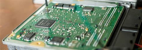
Assembly pcb
Understanding The Basics Of PCB Assembly
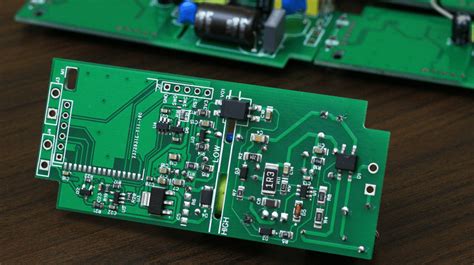
Printed Circuit Board (PCB) assembly is a critical process in the manufacturing of electronic devices, serving as the backbone that supports and connects various electronic components. Understanding the basics of PCB assembly is essential for anyone involved in electronics design and production. This process involves several stages, each requiring precision and attention to detail to ensure the functionality and reliability of the final product.
Initially, the process begins with the design phase, where engineers create a schematic diagram of the circuit.
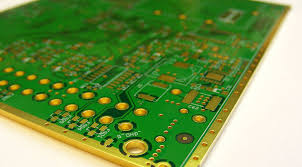
This schematic serves as a blueprint, guiding the placement of components on the board. Once the design is finalized, it is converted into a layout using specialized software. This layout specifies the exact positioning of components and the routing of electrical connections, known as traces, on the board. The design is then sent to a manufacturer to produce the physical PCB, which consists of multiple layers of conductive and insulating materials laminated together.
Following the production of the PCB, the assembly process commences with the application of solder paste.
This paste, a mixture of powdered solder and flux, is applied to the board using a stencil that matches the layout of the pads where components will be placed. The solder paste serves as an adhesive, temporarily holding components in place and providing the necessary material for creating permanent electrical connections.
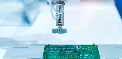
Subsequently, components are placed onto the board using automated machines known as pick-and-place machines.
These machines are programmed to accurately position each component according to the design layout. The components used in PCB assembly can be broadly categorized into two types: surface-mount devices (SMDs) and through-hole components. SMDs are mounted directly onto the surface of the board, while through-hole components have leads that pass through holes in the board and are soldered on the opposite side.
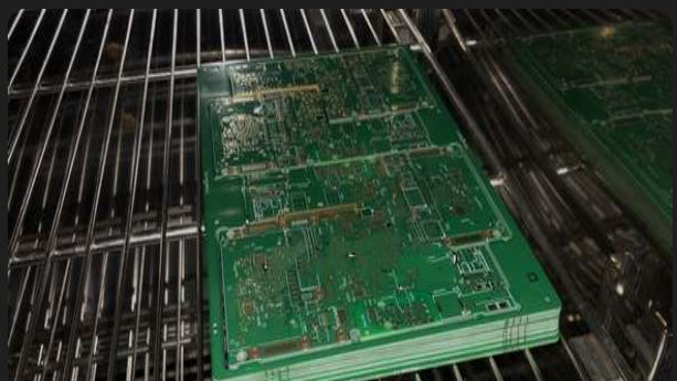
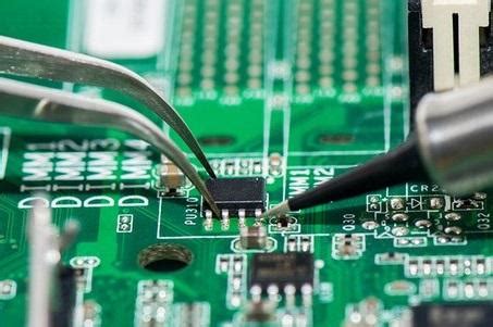
Once all components are placed, the board undergoes a reflow soldering process.
During this stage, the board is passed through a reflow oven, where it is gradually heated to melt the solder paste. As the solder cools, it solidifies, forming strong electrical connections between the components and the board. For through-hole components, an additional soldering process called wave soldering may be used, where the board is passed over a wave of molten solder to ensure proper connection.
After soldering, the assembled PCB is subjected to inspection and testing to verify its functionality.
Automated optical inspection (AOI) systems are commonly used to check for defects such as misaligned components or soldering issues. Additionally, functional testing is performed to ensure that the board operates as intended. This may involve applying power to the board and checking for correct output signals or using specialized test equipment to simulate real-world operating conditions.
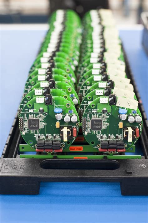
In conclusion, PCB assembly is a complex process that requires careful planning and execution. From the initial design to the final testing, each step is crucial in ensuring the production of high-quality electronic devices. As technology continues to advance, the demand for more sophisticated and reliable PCBs will only increase, making a thorough understanding of PCB assembly processes more important than ever for professionals in the electronics industry.
Key Challenges In PCB Assembly And How To Overcome Them
Printed Circuit Board (PCB) assembly is a critical process in the electronics manufacturing industry, serving as the backbone for a wide array of electronic devices. However, this process is fraught with numerous challenges that can impact the quality, efficiency, and cost-effectiveness of the final product. Understanding these challenges and implementing strategies to overcome them is essential for manufacturers aiming to maintain competitive advantage and ensure product reliability.
One of the primary challenges in PCB assembly is the increasing complexity of designs.
As electronic devices become more sophisticated, PCBs must accommodate a higher density of components, often in smaller form factors. This complexity can lead to difficulties in component placement and soldering, increasing the risk of defects such as solder bridges or misaligned components. To address this, manufacturers can invest in advanced assembly equipment that offers higher precision and automation capabilities. Additionally, employing design for manufacturability (DFM) principles during the design phase can help mitigate these issues by ensuring that the PCB layout is optimized for efficient assembly.
Another significant challenge is the management of component variability and supply chain disruptions.
The global electronics supply chain is susceptible to fluctuations in component availability, which can lead to delays and increased costs. To overcome this, manufacturers should establish strong relationships with multiple suppliers to ensure a steady supply of components. Furthermore, implementing a robust inventory management system can help track component usage and forecast future needs, reducing the impact of supply chain disruptions.
Quality control is also a critical concern in PCB assembly.
Defects in PCBs can lead to device failures, which can be costly and damage a manufacturer’s reputation. To enhance quality control, manufacturers can adopt automated optical inspection (AOI) and X-ray inspection technologies. These tools allow for the rapid detection of defects, such as solder joint issues or component misalignments, enabling timely corrective actions. Moreover, implementing a comprehensive testing protocol, including in-circuit testing (ICT) and functional testing, can further ensure the reliability of the assembled PCBs.
Thermal management presents another challenge, particularly as devices become more compact and power-dense.
Excessive heat can lead to component failure and reduced device lifespan. To address thermal management issues, manufacturers can incorporate thermal vias, heat sinks, and other cooling solutions into the PCB design. Additionally, selecting materials with high thermal conductivity for the PCB substrate can help dissipate heat more effectively.
Finally, the push for environmental sustainability is increasingly influencing PCB assembly processes.
Manufacturers are under pressure to reduce waste and energy consumption while complying with environmental regulations such as the Restriction of Hazardous Substances (RoHS) directive. To meet these demands, companies can adopt lead-free soldering techniques and explore the use of recyclable materials in PCB production. Furthermore, optimizing assembly processes to minimize energy use and waste generation can contribute to a more sustainable manufacturing operation.
In conclusion, while PCB assembly presents several challenges, manufacturers can overcome these obstacles through strategic investments in technology, process optimization, and supply chain management. By addressing design complexity, component variability, quality control, thermal management, and sustainability, companies can enhance their assembly processes, ensuring the production of high-quality, reliable PCBs that meet the demands of today’s electronics market.
Innovations In PCB Assembly Technology
Printed Circuit Board (PCB) assembly technology has undergone significant advancements in recent years, driven by the increasing demand for more efficient, compact, and reliable electronic devices. As the backbone of modern electronics, PCBs are integral to the functionality of a wide array of products, from consumer electronics to industrial machinery. Consequently, innovations in PCB assembly technology are crucial for meeting the evolving needs of various industries.
One of the most notable advancements in PCB assembly is the development of surface mount technology (SMT).
SMT has revolutionized the way components are mounted onto PCBs, allowing for smaller and more densely packed boards. This technology replaces the traditional through-hole mounting method, which required drilling holes into the board for component leads. By contrast, SMT components are directly mounted onto the surface of the PCB, significantly reducing the size and weight of the final product. This innovation not only enhances the performance of electronic devices but also reduces manufacturing costs and time.
In addition to SMT, the introduction of automated assembly processes has further transformed PCB manufacturing.
Automation has enabled manufacturers to achieve higher precision and consistency in PCB assembly, minimizing human error and increasing production efficiency. Robotic systems equipped with advanced vision and placement technologies can accurately position components on the board at high speeds, ensuring that even the most complex designs are assembled with precision. This level of automation is particularly beneficial for high-volume production, where consistency and speed are paramount.
Moreover, the advent of advanced materials and fabrication techniques has also played a significant role in the evolution of PCB assembly technology.
For instance, the use of flexible PCBs has gained popularity due to their ability to bend and conform to various shapes, making them ideal for applications where space is limited or where the board must fit into unconventional enclosures. Flexible PCBs are commonly used in wearable technology, medical devices, and automotive applications, where their adaptability and durability offer distinct advantages.
Furthermore, the integration of advanced testing and inspection methods has enhanced the reliability of PCB assemblies.
Techniques such as automated optical inspection (AOI) and X-ray inspection allow manufacturers to detect defects and ensure the quality of the assembled boards. These methods provide a non-destructive means of verifying the integrity of solder joints and component placements, thereby reducing the likelihood of failures in the field. As a result, manufacturers can deliver products that meet stringent quality standards and customer expectations.
In parallel with these technological advancements, the push for environmentally friendly manufacturing practices has also influenced PCB assembly processes.
The adoption of lead-free soldering techniques, driven by regulatory requirements and consumer demand for sustainable products, has become a standard practice in the industry. Lead-free solders, typically composed of tin, silver, and copper, offer a safer alternative to traditional lead-based solders while maintaining the necessary mechanical and electrical properties.
In conclusion, innovations in PCB assembly technology have significantly enhanced the capabilities and efficiency of electronic manufacturing.
From surface mount technology and automation to advanced materials and inspection methods, these advancements have enabled the production of smaller, more reliable, and environmentally friendly electronic devices. As technology continues to evolve, it is likely that further innovations will emerge, driving the PCB assembly industry toward even greater levels of sophistication and performance.

Best Practices For Quality Control In PCB Assembly
In the realm of electronics manufacturing, ensuring the quality of printed circuit board (PCB) assemblies is paramount. The intricate nature of PCBs, which serve as the backbone of electronic devices, necessitates rigorous quality control measures to prevent defects and ensure reliability. Implementing best practices in quality control during PCB assembly not only enhances product performance but also reduces costs associated with rework and returns. To achieve this, manufacturers must adopt a comprehensive approach that encompasses various stages of the assembly process.
Initially, it is crucial to begin with a meticulous design review.
This involves scrutinizing the PCB layout for potential issues such as trace routing, component placement, and thermal management. By addressing these concerns early in the design phase, manufacturers can preemptively mitigate risks that might arise during assembly. Furthermore, employing design for manufacturability (DFM) principles ensures that the PCB design is optimized for efficient and error-free production.
Transitioning from design to production, the selection of high-quality materials and components is another critical factor.
Sourcing components from reputable suppliers and verifying their specifications can significantly reduce the likelihood of defects. Additionally, maintaining a controlled environment for storage and handling of components helps prevent damage and contamination, which could compromise the assembly process.
As the assembly process commences, the implementation of automated inspection systems becomes indispensable.
Automated optical inspection (AOI) and automated X-ray inspection (AXI) are powerful tools that enable the detection of defects such as solder joint issues, component misalignment, and missing components. These systems provide rapid feedback, allowing for immediate corrective actions and minimizing the propagation of errors through subsequent stages.
Moreover, in-process quality control is essential to maintain consistency and reliability.
This involves continuous monitoring of critical parameters such as solder paste application, reflow oven temperature profiles, and placement accuracy. By employing statistical process control (SPC) techniques, manufacturers can identify trends and variations that may indicate potential quality issues, thereby facilitating timely interventions.
In addition to automated inspections, manual inspections play a complementary role in quality control.
Skilled technicians can identify subtle defects that automated systems might overlook, such as cosmetic blemishes or minor mechanical issues. Regular training and certification of inspection personnel ensure that they remain adept at identifying and addressing quality concerns.
Furthermore, functional testing of assembled PCBs is a vital step in verifying their performance.
This involves subjecting the boards to electrical tests that simulate real-world operating conditions. By doing so, manufacturers can confirm that the PCBs meet the required specifications and function as intended. Any deviations detected during testing can be traced back to specific stages in the assembly process, facilitating targeted corrective actions.
Finally, fostering a culture of continuous improvement is essential for sustaining high-quality standards in PCB assembly.
This involves analyzing data from quality control processes to identify areas for enhancement and implementing corrective and preventive actions. Encouraging open communication and collaboration among design, production, and quality assurance teams fosters a proactive approach to quality management.
In conclusion, the pursuit of excellence in PCB assembly quality control requires a holistic strategy that integrates design optimization, material selection, automated and manual inspections, in-process monitoring, and functional testing. By adhering to these best practices, manufacturers can ensure the production of reliable and high-performance PCBs, ultimately contributing to the success and longevity of electronic products