Pcb manufacturing processes
Introduction To PCB Design And Layout
Printed Circuit Boards (PCBs) are the backbone of modern electronic devices, serving as the foundation upon which electronic components are mounted and interconnected. The design and layout of PCBs are critical steps in the manufacturing process, as they determine the functionality, efficiency, and reliability of the final product. Understanding the intricacies of PCB design and layout is essential for engineers and designers who aim to create effective and innovative electronic solutions.
The process of PCB design begins with a clear understanding of the device’s requirements and specifications.
This involves defining the electrical and mechanical constraints, such as the size of the board, the number of layers, and the types of components to be used. Once these parameters are established, designers employ specialized software tools to create a schematic diagram, which serves as a blueprint for the circuit. This schematic outlines the electrical connections between components, ensuring that the circuit will function as intended.
Transitioning from the schematic to the physical layout of the PCB involves several critical considerations.
One of the primary challenges is optimizing the placement of components to minimize signal interference and ensure efficient use of space. Designers must strategically position components to reduce the length of electrical traces, which can help minimize resistance and potential signal degradation. Additionally, careful attention must be paid to the routing of these traces, as improper routing can lead to issues such as crosstalk, electromagnetic interference, and signal reflection.
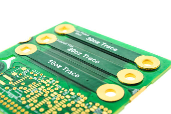
Moreover, the choice of materials and the number of layers in a PCB are crucial factors that influence the design process.
Multilayer PCBs, for instance, allow for more complex circuits by providing additional layers for routing traces, which can be particularly beneficial in high-density applications. However, this complexity comes with increased manufacturing costs and potential challenges in heat dissipation. Therefore, designers must balance these considerations to achieve an optimal design that meets both performance and budgetary constraints.
As the design progresses, simulation and testing become integral components of the process.
Designers use simulation tools to model the electrical behavior of the circuit, allowing them to identify and rectify potential issues before the board is physically manufactured. This step is vital in ensuring that the PCB will perform reliably under various operating conditions. Once the design is finalized, a prototype is typically produced for further testing and validation. This prototype serves as a tangible representation of the design, enabling engineers to conduct real-world tests and make any necessary adjustments.
In conclusion, the design and layout of PCBs are complex processes that require a deep understanding of both electrical engineering principles and practical manufacturing considerations. By carefully planning each step, from schematic creation to prototype testing, designers can create PCBs that not only meet the technical requirements of their projects but also adhere to cost and time constraints. As technology continues to advance, the demand for more sophisticated and efficient PCBs will only grow, underscoring the importance of mastering these foundational skills in the field of electronics. Through continuous learning and adaptation, engineers and designers can ensure that they remain at the forefront of innovation in PCB manufacturing.

Understanding The PCB Fabrication Process
Printed Circuit Boards (PCBs) are the backbone of modern electronic devices, serving as the foundation upon which electronic components are mounted and interconnected. Understanding the PCB fabrication process is crucial for anyone involved in electronics design and manufacturing, as it directly impacts the performance, reliability, and cost of the final product. The process begins with the design phase, where engineers use specialized software to create a schematic diagram and layout of the circuit. This design is then translated into a format suitable for manufacturing, typically a Gerber file, which contains all the necessary information about the board’s layers, traces, and component placements.
Once the design is finalized, the actual fabrication process commences with the selection of the base material, usually a fiberglass-reinforced epoxy laminate known as FR-4.
This material is chosen for its excellent electrical insulation properties and mechanical strength. The next step involves the application of a thin layer of copper to both sides of the substrate, which will form the conductive pathways of the circuit. This copper layer is then coated with a photosensitive film, which plays a critical role in the subsequent photolithography process.
Photo lithography is a pivotal stage in PCB manufacturing, where the board is exposed to ultraviolet light through a mask that represents the circuit pattern.
The light-sensitive film hardens in the exposed areas, creating a protective barrier over the copper. The unexposed areas are then removed using a chemical solution, revealing the underlying copper that needs to be etched away. This etching process removes the unwanted copper, leaving behind the desired circuit pattern. Following etching, the remaining photoresist is stripped away, exposing the copper traces that form the circuit.
To ensure the board’s durability and performance, a solder mask is applied over the entire surface, except for the areas where components will be soldered.
This mask not only protects the copper traces from oxidation and environmental damage but also prevents solder bridges during component assembly. The application of the solder mask is followed by the addition of a silkscreen layer, which provides labels and markings to aid in component placement and troubleshooting.
Drilling is another essential step in PCB fabrication, as it creates the holes necessary for mounting components and establishing electrical connections between different layers of the board. These holes are plated with copper to ensure conductivity, a process known as through-hole plating. For multilayer PCBs, additional layers are laminated together under heat and pressure, with vias drilled and plated to connect the layers electrically.
Finally, the board undergoes a series of inspections and tests to verify its integrity and functionality.
Automated optical inspection (AOI) systems are used to detect any defects in the traces or solder mask, while electrical testing ensures that all connections are correct and that there are no short circuits. Once the board passes these quality checks, it is ready for component assembly and integration into electronic devices.
In conclusion, the PCB fabrication process is a complex and precise series of steps that transform a design into a functional electronic platform. Each stage, from design to final inspection, plays a vital role in ensuring the quality and performance of the finished product. Understanding these processes not only enhances one’s appreciation of modern electronics but also underscores the importance of meticulous planning and execution in PCB manufacturing.
Key Techniques In PCB Assembly
Printed Circuit Board (PCB) assembly is a critical phase in the electronics manufacturing process, where various electronic components are mounted onto a PCB to create a functional electronic device. This process involves several key techniques that ensure the reliability and performance of the final product. Understanding these techniques is essential for anyone involved in electronics design and manufacturing.
To begin with, Surface Mount Technology (SMT) is one of the most prevalent methods used in PCB assembly.
SMT involves placing components directly onto the surface of the PCB, as opposed to inserting them through holes. This technique allows for a higher component density, which is crucial for modern electronic devices that demand compact and efficient designs. The process typically starts with the application of solder paste onto the PCB using a stencil. This is followed by the placement of components using a pick-and-place machine, which ensures precision and speed. Once the components are in place, the board is subjected to a reflow soldering process, where it is heated in a controlled manner to melt the solder paste, creating strong electrical connections.
In contrast, Through-Hole Technology (THT) involves inserting component leads through pre-drilled holes on the PCB.
This method is often used for components that require a stronger mechanical bond, such as connectors or large capacitors. THT is generally considered more robust than SMT, making it suitable for applications where durability is paramount. The soldering process for THT can be manual or automated, with wave soldering being a common technique. In wave soldering, the PCB is passed over a wave of molten solder, which adheres to the exposed metal areas, forming secure connections.
Another critical technique in PCB assembly is the use of Automated Optical Inspection (AOI).
AOI systems are employed to inspect PCBs for defects such as misaligned components, solder bridges, or missing parts. This non-contact method uses cameras and image processing software to detect anomalies, ensuring that only defect-free boards proceed to the next stage of production. AOI is particularly valuable in high-volume manufacturing, where manual inspection would be impractical and error-prone.
Furthermore, the implementation of In-Circuit Testing (ICT) is a vital step in verifying the functionality of assembled PCBs.
ICT involves using a bed of nails tester to make contact with various test points on the PCB. This allows for the measurement of electrical properties such as resistance, capacitance, and signal integrity. ICT can quickly identify issues like short circuits or open connections, providing valuable feedback for quality control.
Finally, the importance of Design for Manufacturability (DFM) cannot be overstated in PCB assembly.
DFM principles guide the design process to ensure that PCBs can be manufactured efficiently and cost-effectively. This involves considering factors such as component placement, trace routing, and thermal management during the design phase. By adhering to DFM guidelines, manufacturers can minimize production costs and reduce the likelihood of defects.
In conclusion, the key techniques in PCB assembly, including SMT, THT, AOI, ICT, and DFM, play a crucial role in the production of reliable and high-performance electronic devices. Each technique offers unique advantages and challenges, and their successful integration is essential for achieving optimal results in PCB manufacturing. As technology continues to evolve, these techniques will undoubtedly adapt to meet the demands of increasingly complex electronic designs.
Quality Control And Testing In PCB Manufacturing
In the realm of printed circuit board (PCB) manufacturing, quality control and testing are pivotal components that ensure the reliability and functionality of the final product. As PCBs serve as the backbone of electronic devices, any defects or failures can lead to significant malfunctions, underscoring the importance of rigorous quality assurance processes. To achieve this, manufacturers employ a variety of testing methodologies and quality control measures throughout the production cycle.
Initially, the quality control process begins with the inspection of raw materials.
Ensuring that the substrates, copper foils, and other essential materials meet specified standards is crucial. This preliminary step helps in mitigating potential issues that could arise later in the manufacturing process. Once the materials are verified, the focus shifts to the fabrication stage, where precision is paramount. During this phase, manufacturers utilize advanced imaging and laser technologies to ensure that the etching and layering of the PCB are executed with exactitude. Any deviations from the design specifications are promptly identified and rectified.
As the PCB progresses through the manufacturing stages, automated optical inspection (AOI) systems play a critical role.
These systems employ high-resolution cameras and sophisticated algorithms to detect defects such as misalignments, shorts, and open circuits. By providing real-time feedback, AOI systems enable manufacturers to address issues immediately, thereby reducing the likelihood of defective boards reaching the final stages of production. Furthermore, AOI is complemented by electrical testing, which involves checking the continuity and isolation of the circuits. This step is essential in verifying that the electrical pathways function as intended.
In addition to these automated processes, manual inspections are also conducted to ensure comprehensive quality control.
Skilled technicians examine the PCBs for any physical defects that machines might overlook, such as surface blemishes or incomplete solder joints. This human element adds an additional layer of scrutiny, enhancing the overall reliability of the quality control process.
Once the PCBs are assembled, functional testing is performed to simulate real-world operating conditions.
This involves subjecting the boards to various stress tests, including thermal cycling and vibration testing, to assess their durability and performance under different environmental conditions. Such rigorous testing ensures that the PCBs can withstand the demands of their intended applications, whether in consumer electronics, automotive systems, or aerospace technologies.
Moreover, manufacturers often implement statistical process control (SPC) techniques to monitor and control the production process. By analyzing data collected during manufacturing, SPC helps in identifying trends and variations that could indicate potential quality issues. This proactive approach allows manufacturers to make informed adjustments to the process, thereby maintaining consistent quality standards.
In conclusion, quality control and testing in PCB manufacturing are integral to producing reliable and high-performance electronic components. Through a combination of advanced technologies, manual inspections, and statistical analysis, manufacturers can ensure that their products meet the stringent requirements of modern electronic applications. As technology continues to evolve, the importance of robust quality control measures in PCB manufacturing will only grow, reinforcing the need for continuous innovation and improvement in testing methodologies.