Online pcb design and manufacture
Innovations In Online PCB Design Tools
The landscape of printed circuit board (PCB) design and manufacture has undergone a significant transformation with the advent of online tools, which have introduced a new era of accessibility and efficiency. These innovations in online PCB design tools have not only democratized the design process but also streamlined the manufacturing pipeline, making it easier for both seasoned engineers and hobbyists to bring their electronic projects to life. As we delve into the intricacies of these advancements, it becomes evident that the integration of sophisticated features and user-friendly interfaces has played a pivotal role in reshaping the industry.
To begin with, one of the most notable innovations in online PCB design tools is the incorporation of cloud-based platforms.
These platforms allow users to access their projects from any location, facilitating collaboration among team members who may be dispersed across different geographical regions. This capability is particularly beneficial in today’s globalized world, where remote work and virtual teams are becoming increasingly common. Moreover, cloud-based tools often come with automatic updates, ensuring that users always have access to the latest features and improvements without the need for manual installations.
In addition to cloud integration, the rise of artificial intelligence (AI) and machine learning has further enhanced the capabilities of online PCB design tools.
AI-driven algorithms can now assist designers by suggesting optimal component placements and routing paths, thereby reducing the likelihood of errors and improving the overall efficiency of the design process. These intelligent systems can analyze vast amounts of data to provide insights that would be difficult for a human designer to discern, ultimately leading to more reliable and high-performance PCBs.
Furthermore, the user interfaces of online PCB design tools have become increasingly intuitive, lowering the barrier to entry for individuals who may not have extensive experience in electronics design. Drag-and-drop functionalities, real-time simulations, and interactive tutorials are just a few examples of how these tools cater to users of varying skill levels. By simplifying complex processes, these innovations empower a broader audience to engage in PCB design, fostering a culture of innovation and creativity.
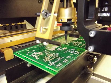
Another significant advancement is the seamless integration of design and manufacturing processes
. Many online PCB design tools now offer direct links to manufacturing services, allowing users to transition from design to production with minimal effort. This integration not only saves time but also reduces the potential for errors that can occur when transferring files between different platforms. By providing a cohesive ecosystem, these tools ensure that the final product accurately reflects the designer’s intentions.
Moreover, the cost-effectiveness of online PCB design tools cannot be overlooked.
Traditional PCB design software often requires substantial financial investment, which can be prohibitive for small businesses and individual creators. In contrast, many online tools offer flexible pricing models, including free versions with basic features and subscription-based plans for more advanced capabilities. This affordability makes high-quality PCB design accessible to a wider audience, encouraging innovation and experimentation.
In conclusion, the innovations in online PCB design tools have revolutionized the way electronic projects are conceived and executed. Through cloud-based platforms, AI integration, user-friendly interfaces, seamless manufacturing links, and cost-effective solutions, these tools have made PCB design more accessible, efficient, and reliable than ever before. As technology continues to evolve, it is likely that we will witness even more groundbreaking developments in this field, further enhancing the capabilities and reach of online PCB design and manufacture.
Streamlining PCB Manufacturing With Online Platforms
In recent years, the field of printed circuit board (PCB) design and manufacturing has undergone a significant transformation, largely due to the advent of online platforms. These platforms have streamlined the process, making it more accessible and efficient for engineers and hobbyists alike. Traditionally, PCB design and manufacturing involved a complex series of steps, often requiring specialized software and a deep understanding of the intricacies involved in circuit design. However, with the rise of online platforms, this process has become more user-friendly and integrated, allowing for a seamless transition from design to production.
One of the primary advantages of using online platforms for PCB design is the accessibility they offer.
These platforms typically provide intuitive interfaces that guide users through the design process, often with drag-and-drop features and extensive libraries of components. This ease of use significantly lowers the barrier to entry, enabling individuals with varying levels of expertise to engage in PCB design. Moreover, many platforms offer tutorials and community support, further enhancing the learning experience and fostering a collaborative environment.
In addition to accessibility, online PCB design platforms offer a high degree of flexibility.
Users can experiment with different design configurations and instantly see the impact of their changes. This real-time feedback is invaluable, as it allows designers to iterate quickly and efficiently, ultimately leading to more refined and optimized designs. Furthermore, these platforms often include simulation tools that enable users to test their circuits virtually before committing to physical production. This capability not only saves time but also reduces the risk of costly errors.
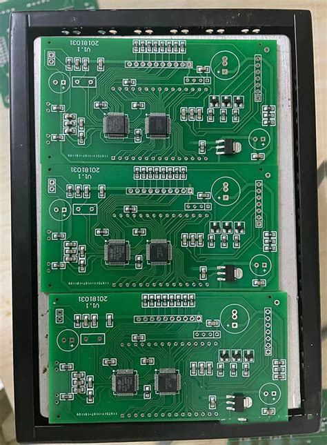
Once the design phase is complete, online platforms facilitate a smooth transition to manufacturing.
Many platforms are integrated with PCB fabrication services, allowing users to submit their designs directly for production. This integration eliminates the need for manual file transfers and reduces the potential for errors during the handoff between design and manufacturing. Additionally, online platforms often provide instant quotes and lead time estimates, enabling users to make informed decisions about their projects.
The benefits of online PCB manufacturing extend beyond convenience and efficiency.
These platforms often leverage economies of scale, offering competitive pricing that is particularly advantageous for small-scale production runs. This cost-effectiveness is further enhanced by the ability to order prototypes in small quantities, allowing designers to test and refine their products without committing to large production volumes. As a result, online platforms empower innovators to bring their ideas to market more quickly and with less financial risk.
Moreover, the global reach of online PCB platforms opens up new opportunities for collaboration and innovation.
Designers from different parts of the world can easily share their projects and insights, leading to a cross-pollination of ideas and techniques. This interconnectedness not only accelerates the pace of innovation but also fosters a sense of community among PCB designers and manufacturers.
In conclusion, the emergence of online platforms for PCB design and manufacturing has revolutionized the industry by making it more accessible, flexible, and efficient. These platforms have democratized the process, enabling a wider range of individuals to participate in PCB design and production. As technology continues to advance, it is likely that these platforms will become even more sophisticated, further streamlining the process and opening up new possibilities for innovation in the field of electronics.

Cost-Effective Strategies For Online PCB Prototyping
In the rapidly evolving landscape of electronics, the demand for efficient and cost-effective printed circuit board (PCB) prototyping has never been higher. As technology advances, so does the need for innovative solutions that streamline the design and manufacturing processes. Online PCB design and manufacturing platforms have emerged as a pivotal resource, offering a range of strategies to reduce costs while maintaining high-quality standards. By leveraging these platforms, engineers and designers can optimize their workflows, minimize expenses, and accelerate the development cycle.
One of the primary cost-effective strategies for online PCB prototyping is the utilization of design software that is both powerful and accessible.
Many online platforms provide free or low-cost design tools that are equipped with advanced features, enabling users to create intricate PCB layouts without the need for expensive software licenses. These tools often include libraries of pre-designed components, which can significantly reduce the time and effort required to develop a new design from scratch. By using these resources, designers can focus on innovation and functionality rather than being bogged down by the complexities of the design process.
In addition to software, online platforms offer a variety of services that can further reduce costs.
For instance, many companies provide instant quoting systems that allow users to quickly estimate the cost of manufacturing their designs. This transparency in pricing helps designers make informed decisions about their projects, enabling them to adjust specifications to meet budgetary constraints. Furthermore, some platforms offer tiered pricing models based on order volume, which can lead to significant savings for larger production runs. By taking advantage of these pricing structures, businesses can scale their operations more efficiently.
Another strategy to consider is the use of online design rule checks (DRC) and electrical rule checks (ERC).
These automated tools help identify potential design errors before the manufacturing process begins, reducing the likelihood of costly revisions and rework. By catching issues early in the design phase, engineers can ensure that their prototypes are both functional and manufacturable, ultimately saving time and resources. Moreover, many online platforms offer real-time collaboration features, allowing teams to work together seamlessly regardless of their physical location. This collaborative approach not only enhances the design process but also fosters innovation and creativity.
Furthermore, the integration of rapid prototyping services into online platforms has revolutionized the way PCBs are manufactured.
By offering quick turnaround times and low minimum order quantities, these services enable designers to test and iterate their designs more frequently. This iterative approach allows for the identification and resolution of issues at an early stage, reducing the risk of costly errors in the final product. Additionally, the ability to produce small batches of prototypes means that designers can experiment with different materials and technologies without incurring significant expenses.
In conclusion, the advent of online PCB design and manufacturing platforms has introduced a multitude of cost-effective strategies for prototyping. By leveraging accessible design software, transparent pricing models, automated design checks, and rapid prototyping services, engineers and designers can optimize their workflows and reduce expenses. These platforms not only facilitate the efficient development of high-quality PCBs but also empower innovators to bring their ideas to life with greater speed and precision. As the electronics industry continues to evolve, embracing these strategies will be crucial for staying competitive in a dynamic market.
Enhancing Collaboration In Online PCB Design Projects
In the rapidly evolving landscape of technology, the design and manufacture of printed circuit boards (PCBs) have undergone significant transformations, particularly with the advent of online platforms. These platforms have not only streamlined the design process but have also enhanced collaboration among engineers, designers, and manufacturers. As the demand for more complex and efficient electronic devices grows, the need for effective collaboration in PCB design projects becomes increasingly critical. Online PCB design tools have emerged as a pivotal solution, offering a range of features that facilitate seamless teamwork and communication.
One of the primary advantages of online PCB design platforms is their ability to provide real-time collaboration.
Unlike traditional methods, where design files are exchanged via email or other means, online platforms allow multiple users to work on the same project simultaneously. This real-time interaction ensures that all team members are on the same page, reducing the likelihood of errors and miscommunications. Moreover, these platforms often include version control features, which enable users to track changes, revert to previous versions, and maintain a comprehensive history of the project’s development. This not only enhances transparency but also fosters a more organized workflow.
Furthermore, online PCB design tools often come equipped with integrated communication features, such as chat functions and comment sections.
These tools allow team members to discuss design elements, share feedback, and resolve issues without leaving the platform. This integration of communication within the design environment minimizes disruptions and keeps the focus on the project at hand. Additionally, the ability to annotate designs directly within the platform ensures that feedback is contextually relevant and easily accessible to all team members.
Another significant benefit of online PCB design platforms is their accessibility.
With cloud-based solutions, team members can access the design project from anywhere in the world, provided they have an internet connection. This is particularly advantageous for teams that are geographically dispersed, as it eliminates the need for physical presence and allows for a more flexible working arrangement. Consequently, companies can tap into a global talent pool, bringing together experts from different regions to collaborate on a single project. This diversity of expertise can lead to more innovative solutions and a higher quality end product.
In addition to enhancing collaboration among team members, online PCB design platforms also facilitate better communication with manufacturers.
Many of these platforms offer features that allow designers to share their projects directly with manufacturing partners, ensuring that the transition from design to production is as smooth as possible. This direct line of communication helps to identify potential manufacturing issues early in the process, reducing the risk of costly revisions and delays. Moreover, some platforms provide design for manufacturability (DFM) analysis tools, which automatically check the design against manufacturing constraints and provide recommendations for optimization.
In conclusion, the integration of online PCB design tools into the workflow of electronic design projects has significantly enhanced collaboration among team members and with manufacturing partners. By providing real-time collaboration, integrated communication features, and global accessibility, these platforms have revolutionized the way PCB design projects are executed. As technology continues to advance, it is likely that these tools will become even more sophisticated, further streamlining the design process and fostering innovation in the field of electronics.