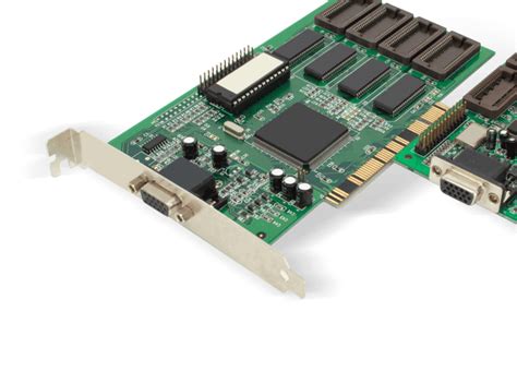
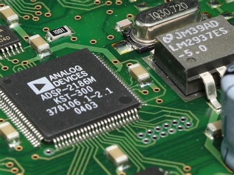
Multilayer pcb stackup planning
Importance Of Multilayer PCB Stackup In Modern Electronics
In the rapidly evolving landscape of modern electronics, the importance of multilayer PCB stackup planning cannot be overstated. As electronic devices become increasingly complex and compact, the demand for efficient and reliable printed circuit boards (PCBs) has surged. Multilayer PCBs, which consist of multiple layers of conductive material separated by insulating layers, have emerged as a critical component in meeting these demands. The stackup of these layers plays a pivotal role in determining the performance, reliability, and manufacturability of the final product.
To begin with, the stackup design of a multilayer PCB significantly influences its electrical performance.
By carefully planning the arrangement of signal, power, and ground layers, engineers can optimize signal integrity and minimize electromagnetic interference (EMI). This is particularly crucial in high-speed digital circuits, where signal integrity issues can lead to data corruption and system failures. A well-designed stackup ensures that signals are transmitted with minimal distortion and crosstalk, thereby enhancing the overall performance of the electronic device.
Moreover, the thermal management of a PCB is another critical aspect that is directly impacted by stackup planning.
As electronic components become more powerful, they generate more heat, which must be effectively dissipated to prevent overheating and ensure longevity. A strategically planned stackup can facilitate efficient heat dissipation by incorporating thermal vias and optimizing the placement of power and ground planes. This not only enhances the thermal performance of the PCB but also contributes to the reliability and durability of the electronic device.
In addition to electrical and thermal considerations, mechanical stability is another factor that underscores the importance of multilayer PCB stackup planning.
The choice of materials and the arrangement of layers can significantly affect the mechanical properties of the PCB, such as its rigidity and resistance to bending. A robust stackup design can prevent mechanical failures, such as warping or delamination, which can occur during manufacturing or operation. This is particularly important in applications where the PCB is subjected to mechanical stress or extreme environmental conditions.
Furthermore, the manufacturability of a multilayer PCB is heavily influenced by its stackup design.
A well-planned stackup can simplify the manufacturing process, reduce production costs, and improve yield rates. For instance, by minimizing the number of layers and optimizing the placement of vias, engineers can streamline the fabrication process and reduce the likelihood of defects. This not only enhances the efficiency of production but also ensures that the final product meets the desired quality standards.
In conclusion, the importance of multilayer PCB stackup planning in modern electronics is multifaceted, encompassing electrical performance, thermal management, mechanical stability, and manufacturability. As electronic devices continue to evolve, the demand for sophisticated and reliable PCBs will only increase. By prioritizing stackup planning, engineers can ensure that their designs meet the stringent requirements of modern applications, paving the way for the development of innovative and high-performance electronic products. As such, multilayer PCB stackup planning remains a cornerstone of successful electronic design and manufacturing, underscoring its critical role in the advancement of technology.
Key Considerations For Effective Multilayer PCB Stackup Design
In the realm of electronics design, multilayer printed circuit boards (PCBs) have become indispensable due to their ability to support complex circuitry within a compact form factor. The stackup design of a multilayer PCB is a critical aspect that significantly influences the board’s performance, reliability, and manufacturability. Therefore, understanding the key considerations for effective multilayer PCB stackup planning is essential for engineers and designers aiming to optimize their designs.
To begin with, the number of layers in a PCB stackup is a fundamental consideration.
The decision on the number of layers is primarily driven by the complexity of the circuit, the need for signal integrity, and the constraints of the physical space. A higher number of layers can accommodate more routing channels and power planes, which is beneficial for high-density designs. However, it also increases the cost and complexity of manufacturing. Thus, striking a balance between the number of layers and the design requirements is crucial.
Transitioning to the arrangement of layers, it is important to strategically position signal, power, and ground layers to minimize electromagnetic interference (EMI) and ensure signal integrity.
Typically, ground and power planes are placed adjacent to signal layers to provide a return path for signals, which helps in reducing EMI and crosstalk. Moreover, maintaining symmetry in the stackup is vital to prevent warping during the manufacturing process. Symmetrical stackups ensure even distribution of stress across the board, thereby enhancing its structural integrity.
Another key consideration is the selection of materials for the PCB stackup.
The choice of materials affects the board’s thermal performance, dielectric properties, and overall durability. High-frequency applications, for instance, require materials with low dielectric constant and loss tangent to minimize signal loss. Additionally, thermal management is a critical aspect, especially for boards that operate in high-temperature environments. Using materials with good thermal conductivity can help dissipate heat effectively, thereby improving the board’s reliability.
Furthermore, the thickness of the PCB and its individual layers is an important factor that influences the board’s electrical and mechanical properties.
The overall thickness of the PCB affects its flexibility and the ability to withstand mechanical stress. Meanwhile, the thickness of individual layers, particularly the copper layers, impacts the current-carrying capacity and impedance of the traces. Therefore, careful consideration of layer thickness is necessary to meet the electrical and mechanical requirements of the design.
In addition to these technical considerations, manufacturability is a crucial aspect of multilayer PCB stackup planning.
Designers must collaborate closely with manufacturers to ensure that the stackup design is feasible and cost-effective to produce. This involves understanding the capabilities and limitations of the manufacturing process, such as the minimum trace width and spacing, the aspect ratio of vias, and the tolerances for layer alignment. By aligning the design with manufacturing capabilities, designers can avoid costly redesigns and ensure a smooth production process.
In conclusion, effective multilayer PCB stackup planning requires a comprehensive understanding of various factors, including the number of layers, layer arrangement, material selection, layer thickness, and manufacturability. By carefully considering these aspects, designers can create PCB stackups that meet the performance, reliability, and cost requirements of their applications. As technology continues to advance, the importance of meticulous stackup planning will only grow, underscoring its role as a cornerstone of successful PCB design.
Common Mistakes To Avoid In Multilayer PCB Stackup Planning
In the intricate world of electronics design, multilayer PCB stackup planning is a critical process that demands precision and foresight. However, even seasoned engineers can fall prey to common mistakes that can compromise the functionality and reliability of the final product. Understanding these pitfalls is essential to ensure a successful design and manufacturing process.
One prevalent mistake in multilayer PCB stackup planning is the inadequate consideration of signal integrity.
Designers often overlook the importance of maintaining controlled impedance throughout the board. This oversight can lead to signal degradation, increased electromagnetic interference (EMI), and ultimately, a malfunctioning device. To avoid this, it is crucial to carefully plan the layer arrangement, ensuring that signal layers are properly shielded by ground planes. Additionally, maintaining consistent dielectric thickness and using appropriate materials can significantly enhance signal integrity.
Another common error is the improper allocation of power and ground layers.
Designers sometimes fail to dedicate sufficient layers for power distribution, leading to voltage drops and increased noise. To mitigate this, it is advisable to allocate separate layers for power and ground, ensuring a low-impedance path for current flow. This not only stabilizes the power supply but also reduces the risk of crosstalk between signal layers. Furthermore, employing a symmetrical stackup can help balance mechanical stresses, reducing the likelihood of warping during the manufacturing process.
Thermal management is another critical aspect that is often underestimated in multilayer PCB stackup planning.
Inadequate thermal considerations can result in overheating, affecting the performance and lifespan of the components. To address this, designers should strategically place thermal vias and consider the use of thermal reliefs to facilitate heat dissipation. Additionally, selecting materials with appropriate thermal conductivity can further enhance the board’s ability to manage heat effectively.
Transitioning to the topic of manufacturability, it is essential to recognize that complex stackups can pose significant challenges during fabrication.
Designers sometimes create overly intricate designs that are difficult to manufacture, leading to increased costs and potential delays. To avoid this, it is important to collaborate closely with manufacturers during the design phase, ensuring that the stackup is within their capabilities. Simplifying the design where possible and adhering to standard manufacturing practices can greatly enhance the feasibility of the project.
Moreover, neglecting to perform thorough simulations and testing is a mistake that can have far-reaching consequences.
Relying solely on theoretical calculations without validating the design through simulations can result in unforeseen issues during production. By utilizing simulation tools, designers can identify potential problems early in the design process, allowing for timely adjustments. This proactive approach not only saves time and resources but also ensures a more robust final product.
Lastly, communication breakdowns between design teams and manufacturers can lead to misunderstandings and errors in the stackup planning process.
It is imperative to maintain clear and open lines of communication, ensuring that all parties are aligned on the design specifications and requirements. Regular meetings and reviews can help identify potential issues early, facilitating a smoother transition from design to production.
In conclusion, multilayer PCB stackup planning is a complex process that requires careful attention to detail. By avoiding common mistakes such as neglecting signal integrity, improper power and ground allocation, inadequate thermal management, and overlooking manufacturability, designers can significantly enhance the success of their projects. Additionally, leveraging simulations and maintaining effective communication with manufacturers are crucial steps in ensuring a reliable and efficient final product. Through meticulous planning and collaboration, the challenges of multilayer PCB stackup planning can be effectively navigated, leading to innovative and high-performing electronic devices.

Advanced Techniques For Optimizing Multilayer PCB Stackup Performance
In the realm of electronics design, the optimization of multilayer PCB stackup performance is a critical aspect that can significantly influence the functionality and reliability of the final product. As electronic devices become increasingly complex, the demand for sophisticated multilayer PCBs has surged, necessitating advanced techniques in stackup planning. A well-optimized stackup not only enhances electrical performance but also ensures mechanical stability and thermal management, which are crucial for the longevity and efficiency of electronic devices.
To begin with, understanding the fundamental principles of multilayer PCB stackup is essential.
A stackup refers to the arrangement of conductive and insulating layers within a PCB. The primary goal of stackup planning is to minimize electromagnetic interference (EMI), reduce crosstalk, and ensure signal integrity. By carefully selecting the sequence and materials of these layers, designers can achieve optimal electrical performance. For instance, placing power and ground planes adjacent to each other can create a low-inductance path, which is beneficial for high-speed signal transmission.
Moreover, the choice of materials plays a pivotal role in stackup optimization.
The dielectric constant and loss tangent of the insulating materials can affect signal speed and attenuation. Therefore, selecting materials with appropriate electrical properties is crucial for maintaining signal integrity, especially in high-frequency applications. Additionally, the thermal properties of these materials must be considered to ensure effective heat dissipation, which is vital for preventing overheating and ensuring the reliability of the PCB.
Transitioning to the layout considerations, the arrangement of signal layers within the stackup is another critical factor.
High-speed signals should be routed on inner layers sandwiched between ground planes to shield them from external noise and reduce EMI. This configuration, often referred to as a stripline, provides a controlled impedance environment, which is essential for maintaining signal quality. Furthermore, differential pairs should be routed symmetrically and with consistent spacing to minimize skew and maintain signal integrity.
Another advanced technique involves the use of blind and buried vias, which can enhance the routing density and reduce the number of layers required in a PCB.
By connecting only specific layers, these vias help in optimizing the stackup by minimizing the parasitic inductance and capacitance associated with through-hole vias. However, careful consideration must be given to the manufacturing capabilities and cost implications of using such vias.
In addition to electrical considerations, mechanical and thermal aspects must also be addressed in stackup planning.
The overall thickness of the PCB, determined by the number of layers and the thickness of each layer, affects the mechanical strength and flexibility of the board. A balanced stackup, where the layers are symmetrically arranged around the center, can prevent warping and ensure mechanical stability. Thermal management is equally important, as inadequate heat dissipation can lead to component failure. Incorporating thermal vias and using materials with high thermal conductivity can aid in effective heat management.
In conclusion, optimizing multilayer PCB stackup performance requires a comprehensive approach that considers electrical, mechanical, and thermal factors. By employing advanced techniques such as strategic layer arrangement, careful material selection, and the use of specialized vias, designers can enhance the performance and reliability of multilayer PCBs. As technology continues to evolve, the importance of meticulous stackup planning will only grow, underscoring its significance in the design and development of cutting-edge electronic devices.