Multilayer pcb repair
Techniques For Identifying Faults In Multilayer PCBs
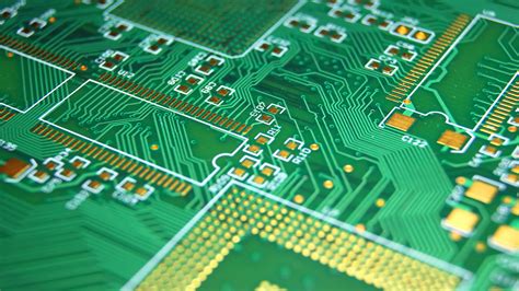
Multilayer printed circuit boards (PCBs) are integral components in modern electronic devices, offering enhanced functionality and compact design. However, their complexity can pose significant challenges when it comes to identifying and repairing faults. Understanding the techniques for identifying faults in multilayer PCBs is crucial for ensuring the reliability and longevity of electronic systems. This article explores various methods and tools that can be employed to effectively diagnose issues in these intricate circuits.
To begin with, visual inspection remains a fundamental technique in fault identification.
Although multilayer PCBs are complex, a thorough visual examination can reveal obvious defects such as burnt components, broken traces, or poor solder joints. Using magnification tools like microscopes can enhance the ability to detect these visible anomalies. However, given the multilayer nature of these PCBs, many faults may be hidden within the internal layers, necessitating more advanced diagnostic techniques.
In addition to visual inspection, electrical testing is a critical method for identifying faults in multilayer PCBs.
Continuity testing, for instance, helps in verifying the electrical connections between different points on the board. By using a multimeter, technicians can check for open circuits or short circuits that may disrupt the board’s functionality. Furthermore, in-circuit testing (ICT) can be employed to assess the performance of individual components while they are still mounted on the board. This method allows for the detection of component-level failures without the need for complete disassembly.
Moreover, advanced diagnostic tools such as X-ray inspection systems provide a non-destructive means of examining the internal layers of a multilayer PCB.
X-ray imaging can reveal hidden defects like voids in solder joints, misaligned layers, or internal shorts that are not visible through traditional inspection methods. This technique is particularly useful for complex boards where internal layers are densely packed with traces and components.
Another sophisticated approach is the use of automated optical inspection (AOI) systems.
AOI employs high-resolution cameras and image processing software to automatically scan the PCB for defects. This method is highly efficient for detecting surface-level issues such as incorrect component placement, soldering defects, and missing components. While AOI is primarily used for surface inspection, it can be combined with other techniques to provide a comprehensive fault diagnosis.
Thermal imaging is also a valuable tool in identifying faults in multilayer PCBs.
By capturing the heat distribution across the board, thermal cameras can pinpoint areas of excessive heat generation, which often indicate faulty components or poor connections. This method is particularly effective in identifying issues related to power distribution and thermal management within the board.
Finally, time-domain reflectometry (TDR) is a specialized technique used to locate faults in the transmission lines of multilayer PCBs.
TDR measures the reflections of electrical signals sent through the board’s traces, allowing technicians to identify discontinuities or impedance mismatches that may cause signal integrity issues.
In conclusion, identifying faults in multilayer PCBs requires a combination of traditional and advanced diagnostic techniques. By employing a systematic approach that includes visual inspection, electrical testing, and the use of sophisticated tools like X-ray and thermal imaging, technicians can effectively diagnose and address issues within these complex circuits. As technology continues to evolve, the development of more precise and efficient diagnostic methods will further enhance the ability to maintain the reliability of multilayer PCBs in electronic devices.
Essential Tools For Multilayer PCB Repair
Repairing multilayer printed circuit boards (PCBs) is a complex task that requires precision, expertise, and the right set of tools. As technology advances, the intricacy of these boards increases, making it essential for technicians to be well-equipped to handle repairs effectively. Understanding the essential tools for multilayer PCB repair is crucial for anyone involved in electronics maintenance and repair.
To begin with, a high-quality soldering station is indispensable.
Unlike single-layer PCBs, multilayer boards require precise temperature control to avoid damaging the delicate internal layers. A soldering station with adjustable temperature settings and a fine-tip soldering iron allows for meticulous work on small components and densely packed areas. Additionally, a hot air rework station is beneficial for desoldering and reflowing components without direct contact, reducing the risk of thermal damage.
Equally important is the use of a microscope or magnification tool.
Multilayer PCBs often feature minute components and intricate traces that are difficult to inspect with the naked eye. A microscope with adequate magnification enables technicians to identify faults, such as broken traces or solder bridges, that could compromise the board’s functionality. Furthermore, it aids in the precise placement and soldering of components, ensuring a reliable repair.
Transitioning to diagnostic tools, a multimeter is essential for testing electrical continuity and verifying the functionality of components.
It allows technicians to measure voltage, current, and resistance, providing valuable insights into the board’s condition. For more advanced diagnostics, an oscilloscope can be employed to analyze signal integrity and detect anomalies in the board’s operation. These tools are crucial for pinpointing issues that may not be immediately visible.
In addition to diagnostic tools, a PCB holder or fixture is necessary to secure the board during repair.
This tool stabilizes the PCB, allowing technicians to work with both hands free, which is particularly important when dealing with multilayer boards that require careful handling. A stable work surface minimizes the risk of accidental damage and enhances the precision of the repair process.
Moreover, the use of high-quality solder and flux cannot be overstated.
Lead-free solder is commonly used due to environmental regulations, but it requires higher temperatures and careful handling. Flux is essential for ensuring good solder flow and preventing oxidation, which can lead to poor connections. Selecting the appropriate solder and flux for the specific board material and components is vital for a successful repair.
Furthermore, a desoldering pump or wick is necessary for removing excess solder and cleaning up solder joints.
These tools help in correcting mistakes and preparing the board for new components. A desoldering pump quickly removes solder by creating a vacuum, while a desoldering wick absorbs solder through capillary action, both of which are invaluable for maintaining clean and functional solder joints.
Finally, an anti-static wrist strap is a simple yet crucial tool for preventing electrostatic discharge (ESD) damage.
Multilayer PCBs are particularly sensitive to ESD, which can irreparably harm components. Wearing an anti-static wrist strap ensures that technicians are grounded, thereby protecting the board from static electricity.
In conclusion, repairing multilayer PCBs demands a comprehensive toolkit that includes soldering and diagnostic equipment, magnification tools, and ESD protection. Each tool plays a vital role in ensuring that repairs are conducted with precision and care, ultimately extending the life and functionality of these complex electronic devices.

Step-By-Step Guide To Repairing Damaged Traces In Multilayer PCBs
Repairing damaged traces in multilayer printed circuit boards (PCBs) is a meticulous process that requires precision and a thorough understanding of the board’s structure. Multilayer PCBs, which consist of multiple layers of conductive traces separated by insulating materials, are integral to modern electronic devices due to their ability to support complex circuitry in a compact form. However, their complexity also makes them susceptible to damage, which can occur due to manufacturing defects, physical stress, or electrical overloads. When a trace is damaged, it can disrupt the entire circuit, necessitating a careful repair process to restore functionality.
The first step in repairing a damaged trace in a multilayer PCB is to accurately diagnose the problem.
This involves visually inspecting the board for any obvious signs of damage, such as burnt areas or broken traces. In cases where the damage is not visible, advanced diagnostic tools like multimeters or oscilloscopes can be employed to test the continuity of the traces and identify the exact location of the fault. Once the damaged trace is identified, it is crucial to document its position and the extent of the damage to ensure a precise repair.
Following the diagnosis, the next step is to prepare the board for repair.
This involves cleaning the affected area to remove any debris or oxidation that may have accumulated. A gentle cleaning solution, such as isopropyl alcohol, can be used along with a soft brush to ensure the area is free from contaminants. It is important to handle the board with care during this process to avoid causing further damage to the delicate traces.
Once the board is prepared, the actual repair of the damaged trace can begin.
This typically involves using a conductive pen or a fine wire to bridge the gap in the trace. Conductive pens contain a special ink that can restore electrical conductivity, while fine wires can be soldered across the break to re-establish the connection. When using a conductive pen, it is essential to apply the ink precisely and allow it to dry completely before testing the board. If opting for a wire, careful soldering is required to ensure a secure and reliable connection without causing short circuits with adjacent traces.
After the repair is completed, it is imperative to test the board to confirm that the trace has been successfully restored.
This involves rechecking the continuity of the trace using a multimeter and powering up the board to ensure that it functions as expected. If the board does not operate correctly, further investigation may be necessary to identify any additional issues or to refine the repair.
In conclusion, repairing damaged traces in multilayer PCBs is a complex task that demands attention to detail and a methodical approach. By accurately diagnosing the problem, preparing the board, and carefully executing the repair, it is possible to restore the functionality of the PCB and extend the life of the electronic device. This process not only requires technical skill but also patience and precision, underscoring the importance of expertise in handling such intricate repairs.

Best Practices For Soldering On Multilayer PCBs
Soldering on multilayer printed circuit boards (PCBs) is a task that demands precision, skill, and a thorough understanding of the complexities involved. Multilayer PCBs, which consist of multiple layers of conductive material separated by insulating layers, are integral to modern electronic devices due to their ability to support complex circuitry in a compact form. However, their intricate design also makes them susceptible to damage during repair processes, particularly when soldering is involved. Therefore, adhering to best practices is essential to ensure successful repairs without compromising the integrity of the board.
To begin with, it is crucial to understand the structure of multilayer PCBs.
These boards typically consist of several layers, including signal layers, power planes, and ground planes, all of which are interconnected through vias. This complexity necessitates a careful approach to soldering, as excessive heat or pressure can easily damage the internal layers or cause delamination. Consequently, the first best practice is to use a temperature-controlled soldering iron. This tool allows for precise temperature settings, minimizing the risk of overheating and ensuring that the solder melts and flows correctly without damaging the board.
In addition to temperature control, selecting the appropriate soldering tip is vital.
A fine-point tip is generally recommended for multilayer PCBs, as it provides better control and access to small components and densely packed areas. Moreover, using a tip that is too large can inadvertently heat surrounding areas, potentially causing unintended damage. Alongside the right tip, employing high-quality solder is equally important. Lead-free solder is often preferred for its environmental benefits, but it requires higher temperatures to melt. Therefore, understanding the specific requirements of the solder being used is essential to avoid cold joints or insufficient solder flow.
Furthermore, the use of flux is a critical component of successful soldering on multilayer PCBs.
Flux helps to clean the surfaces to be soldered, removing oxides and promoting better adhesion of the solder. Applying flux before soldering can significantly enhance the quality of the solder joints, reducing the likelihood of defects such as bridging or incomplete connections. However, it is important to clean any residual flux after soldering, as it can be corrosive and may lead to long-term reliability issues if left on the board.
Another best practice involves the use of magnification tools.
Given the small size and high density of components on multilayer PCBs, visual inspection with the naked eye may not be sufficient. Magnification tools, such as microscopes or magnifying lamps, allow for a detailed examination of the solder joints, ensuring that they are properly formed and free of defects. This step is crucial for identifying any potential issues early in the repair process, thereby preventing more significant problems down the line.
Finally, it is essential to handle multilayer PCBs with care throughout the soldering process. This includes using anti-static wristbands to prevent electrostatic discharge, which can damage sensitive components, and ensuring that the work area is clean and organized to avoid accidental damage. By following these best practices, technicians can effectively repair multilayer PCBs, maintaining their functionality and extending the lifespan of the electronic devices they support. Through careful attention to detail and adherence to these guidelines, the challenges of soldering on multilayer PCBs can be successfully navigated, resulting in reliable and high-quality repairs.