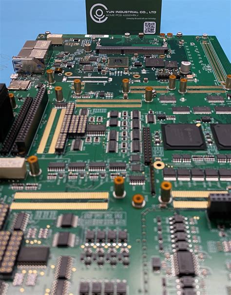
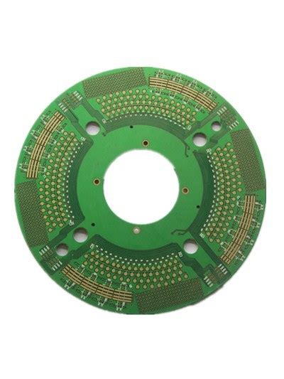
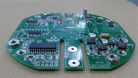
Multilayer pcb inductor
Design Considerations for Multilayer PCB Inductors
In the realm of modern electronics, the design of multilayer printed circuit boards (PCBs) has become increasingly sophisticated, particularly when it comes to integrating components such as inductors. Multilayer PCB inductors are essential in various applications, including power supplies, RF circuits, and signal processing. As technology advances, the demand for compact and efficient electronic devices necessitates careful consideration of several design factors to ensure optimal performance of these inductors.
To begin with, the choice of materials plays a crucial role in the design of multilayer PCB inductors.
The substrate material must possess suitable dielectric properties to support the desired frequency range and minimize losses. Common materials include FR-4, Rogers, and other high-frequency laminates, each offering distinct advantages in terms of dielectric constant, loss tangent, and thermal stability. Selecting the appropriate material is vital to achieving the desired inductance and quality factor (Q-factor) while maintaining the integrity of the signal.
Moreover, the geometry of the inductor is another critical aspect that influences its performance.
The number of turns, spacing between traces, and the width of the traces all contribute to the inductance value and the inductor’s ability to handle current. Designers must carefully balance these parameters to achieve the desired inductance without compromising the inductor’s efficiency or increasing its footprint unnecessarily. Additionally, the use of vias to connect different layers in a multilayer PCB can introduce parasitic inductance and resistance, which must be minimized through strategic placement and design.
Transitioning to the consideration of electromagnetic interference (EMI), it is imperative to address potential issues that may arise from the inductor’s operation.
EMI can significantly affect the performance of nearby components and the overall system. To mitigate these effects, designers often employ shielding techniques or incorporate ground planes within the PCB layout. These measures help to confine the magnetic fields generated by the inductor, thereby reducing the risk of interference with other circuit elements.
Thermal management is another essential consideration in the design of multilayer PCB inductors.
As inductors can generate significant heat during operation, especially in high-power applications, effective heat dissipation is crucial to prevent thermal damage and ensure reliability. This can be achieved through the use of thermal vias, heat sinks, or by optimizing the layout to enhance airflow around the inductor. Proper thermal management not only extends the lifespan of the inductor but also maintains its performance over time.
Furthermore, the integration of multilayer PCB inductors into a design must account for manufacturing tolerances and variability.
The precision of the fabrication process can affect the final inductance value and the inductor’s performance. Therefore, designers should work closely with manufacturers to understand the limitations and capabilities of the production process, allowing for adjustments in the design to accommodate potential variations.
In conclusion, the design of multilayer PCB inductors requires a comprehensive understanding of various factors, including material selection, geometric configuration, EMI considerations, thermal management, and manufacturing constraints. By carefully addressing these elements, designers can create inductors that meet the specific requirements of their applications, ensuring efficient and reliable performance in increasingly complex electronic systems. As technology continues to evolve, the ability to effectively design and integrate multilayer PCB inductors will remain a critical skill in the field of electronics engineering.
Advantages of Using Multilayer PCB Inductors in Modern Electronics
In the rapidly evolving landscape of modern electronics, the demand for compact, efficient, and high-performance components has never been greater. Among these components, multilayer PCB inductors have emerged as a crucial element, offering a range of advantages that cater to the needs of contemporary electronic devices. As technology continues to advance, the role of these inductors becomes increasingly significant, providing solutions that address both current and future challenges in electronic design.
One of the primary advantages of using multilayer PCB inductors is their ability to save space within electronic devices.
As devices become smaller and more complex, the need for miniaturization of components is paramount. Multilayer PCB inductors are designed to stack multiple layers of conductive material, allowing for a more compact form factor compared to traditional single-layer inductors. This compactness not only conserves valuable space on the circuit board but also enables the integration of more components within a limited area, thereby enhancing the overall functionality of the device.
In addition to space-saving benefits, multilayer PCB inductors offer improved electrical performance.
The layered structure of these inductors allows for better control over the inductance value, which is crucial for maintaining signal integrity and reducing electromagnetic interference (EMI). By optimizing the inductance, designers can ensure that the inductor performs efficiently across a wide range of frequencies, making it suitable for various applications, from power supplies to radio frequency (RF) circuits. This versatility is particularly advantageous in the design of multifunctional devices that require reliable performance across different operating conditions.
Furthermore, multilayer PCB inductors contribute to enhanced thermal management within electronic systems.
The compact design and efficient layout of these inductors facilitate better heat dissipation, which is essential for maintaining the stability and longevity of electronic components. Effective thermal management is critical in preventing overheating, which can lead to component failure and reduced device lifespan. By incorporating multilayer PCB inductors, designers can mitigate these risks, ensuring that devices operate within safe temperature ranges even under demanding conditions.
Another notable advantage of multilayer PCB inductors is their cost-effectiveness in mass production.
The manufacturing process for these inductors is highly automated, allowing for consistent quality and reduced production costs. This is particularly beneficial for consumer electronics, where cost efficiency is a key consideration. The ability to produce high-quality inductors at a lower cost enables manufacturers to offer competitive pricing while maintaining the performance standards expected by consumers.
Moreover, the use of multilayer PCB inductors aligns with the growing emphasis on sustainability in electronic design.
The efficient use of materials and the potential for reduced energy consumption contribute to a smaller environmental footprint. As the industry moves towards more sustainable practices, the adoption of components that support these goals becomes increasingly important.
In conclusion, multilayer PCB inductors offer a multitude of advantages that make them indispensable in modern electronics. Their space-saving design, improved electrical performance, enhanced thermal management, cost-effectiveness, and alignment with sustainability goals position them as a key component in the development of next-generation electronic devices. As technology continues to advance, the role of multilayer PCB inductors will undoubtedly expand, driving innovation and enabling the creation of more sophisticated and efficient electronic systems.
Manufacturing Challenges in Multilayer PCB Inductor Production
The production of multilayer PCB inductors presents a unique set of manufacturing challenges that require careful consideration and precise execution. As electronic devices continue to shrink in size while increasing in functionality, the demand for compact and efficient components like multilayer PCB inductors has surged. These components are integral to modern electronics, providing essential inductance in a compact form factor. However, the complexity of their design and manufacturing processes poses significant challenges that manufacturers must overcome to ensure high performance and reliability.
One of the primary challenges in manufacturing multilayer PCB inductors is the precise alignment of multiple layers.
Each layer must be accurately aligned to ensure that the inductor functions correctly. Misalignment can lead to variations in inductance, which can adversely affect the performance of the entire electronic device. To address this issue, manufacturers employ advanced alignment technologies and equipment that can achieve the necessary precision. Additionally, rigorous quality control measures are implemented to detect and correct any misalignments during the production process.
Another significant challenge is the selection of appropriate materials.
The materials used in multilayer PCB inductors must possess specific electrical and thermal properties to ensure optimal performance. For instance, the dielectric material between the layers must have a high dielectric constant to achieve the desired inductance while maintaining a compact size. Moreover, the conductive materials used for the inductor coils must exhibit low resistance to minimize energy losses. Manufacturers must carefully select and test materials to meet these stringent requirements, often necessitating collaboration with material scientists and suppliers.
Thermal management is also a critical concern in the production of multilayer PCB inductors.
As electronic devices become more powerful, they generate more heat, which can affect the performance and longevity of the inductors. Effective thermal management strategies are essential to dissipate heat and prevent overheating. This involves designing the inductor with adequate thermal pathways and using materials with high thermal conductivity. Additionally, manufacturers may incorporate advanced cooling techniques, such as heat sinks or thermal vias, to enhance heat dissipation.
Furthermore, the miniaturization of electronic components adds another layer of complexity to the manufacturing process.
As devices become smaller, the demand for smaller inductors increases, necessitating the development of innovative manufacturing techniques. Manufacturers must employ advanced fabrication technologies, such as laser drilling and precision etching, to produce inductors with fine features and tight tolerances. These techniques require specialized equipment and expertise, adding to the complexity and cost of production.
In addition to these technical challenges, manufacturers must also navigate economic and logistical considerations.
The production of multilayer PCB inductors involves significant investment in equipment, materials, and skilled labor. Moreover, the global supply chain for electronic components can be volatile, with fluctuations in material availability and pricing impacting production schedules and costs. Manufacturers must develop robust supply chain strategies and maintain flexibility to adapt to these challenges.
In conclusion, the production of multilayer PCB inductors is a complex process that involves overcoming numerous technical, economic, and logistical challenges. Manufacturers must employ advanced technologies and materials, implement rigorous quality control measures, and develop effective thermal management strategies to produce high-performance inductors. Despite these challenges, the demand for multilayer PCB inductors continues to grow, driven by the ongoing miniaturization and increased functionality of electronic devices. As a result, manufacturers are continually innovating and refining their processes to meet the evolving needs of the electronics industry.
Applications of Multilayer PCB Inductors in Wireless Communication Systems
Multilayer PCB inductors have become integral components in the realm of wireless communication systems, offering a range of applications that enhance performance and efficiency. As wireless technology continues to evolve, the demand for compact, reliable, and high-performance components has surged, making multilayer PCB inductors increasingly relevant. These inductors are designed by stacking multiple layers of conductive and insulating materials, which allows for a compact design while maintaining the necessary inductance values. This compactness is particularly advantageous in wireless communication systems, where space is often at a premium.
One of the primary applications of multilayer PCB inductors in wireless communication systems is in the design of filters.
Filters are essential in these systems to ensure that signals are transmitted and received without interference from unwanted frequencies. Multilayer PCB inductors are used in conjunction with capacitors to create LC filters, which are crucial for signal integrity. These filters help in minimizing noise and improving the clarity of the transmitted signals, thereby enhancing the overall performance of the communication system. Moreover, the ability to integrate these inductors directly onto the PCB reduces the need for additional components, leading to a more streamlined and efficient design.
In addition to filters, multilayer PCB inductors are also employed in impedance matching networks.
Impedance matching is vital in wireless communication systems to ensure maximum power transfer between components, such as antennas and transmitters. By using multilayer PCB inductors, designers can achieve precise impedance matching, which is critical for maintaining signal strength and reducing power loss. This application is particularly important in mobile devices, where efficient power usage is crucial for extending battery life and improving device performance.
Furthermore, multilayer PCB inductors play a significant role in the design of oscillators and frequency synthesizers.
These components are essential for generating the carrier frequencies used in wireless communication. The stability and precision of these frequencies are paramount, as they directly impact the quality and reliability of the communication link. Multilayer PCB inductors contribute to the stability of oscillators by providing consistent inductance values, which helps maintain the desired frequency over varying environmental conditions. This stability is crucial for applications such as mobile phones, satellite communications, and other wireless devices that require reliable frequency generation.
Another noteworthy application of multilayer PCB inductors is in the development of compact and efficient power amplifiers.
Power amplifiers are responsible for boosting the signal strength before transmission, ensuring that the signal can travel long distances without degradation. The use of multilayer PCB inductors in these amplifiers allows for a reduction in size and weight, which is particularly beneficial for portable wireless devices. Additionally, these inductors contribute to the overall efficiency of the amplifier by minimizing energy losses, thereby enhancing the performance of the communication system.
In conclusion, multilayer PCB inductors are indispensable in the advancement of wireless communication systems. Their applications in filters, impedance matching networks, oscillators, and power amplifiers underscore their versatility and importance. As wireless technology continues to advance, the role of multilayer PCB inductors will likely expand, driven by the ongoing need for compact, efficient, and high-performance components. The integration of these inductors into wireless communication systems not only improves performance but also paves the way for future innovations in the field.