Multilayer ims pcb
Advantages Of Multilayer IMS PCB In Modern Electronics
In the rapidly evolving landscape of modern electronics, the demand for more efficient, compact, and reliable components has never been greater. Among the various innovations that have emerged to meet these demands, multilayer Insulated Metal Substrate (IMS) printed circuit boards (PCBs) stand out as a significant advancement. These sophisticated PCBs offer a range of advantages that make them indispensable in contemporary electronic applications.
To begin with, one of the primary benefits of multilayer IMS PCBs is their exceptional thermal management capabilities.
Traditional PCBs often struggle with heat dissipation, which can lead to performance degradation and reduced lifespan of electronic components. In contrast, IMS PCBs are designed with a metal substrate, typically aluminum or copper, which provides superior thermal conductivity. This allows for efficient heat dissipation away from critical components, thereby enhancing the overall reliability and longevity of the device. As electronic devices become more powerful and compact, effective thermal management becomes crucial, making multilayer IMS PCBs an ideal choice for high-performance applications.
Moreover, the compact nature of multilayer IMS PCBs is another significant advantage.
By integrating multiple layers into a single board, these PCBs can accommodate more complex circuitry without increasing the overall size of the board. This is particularly beneficial in the design of modern electronic devices, where space is often at a premium. The ability to pack more functionality into a smaller footprint not only helps in miniaturizing devices but also contributes to reducing the weight, which is a critical factor in applications such as aerospace and portable consumer electronics.
In addition to their thermal and spatial benefits, multilayer IMS PCBs also offer enhanced electrical performance.
The use of multiple layers allows for more intricate and efficient routing of electrical signals, which can reduce signal interference and improve overall circuit performance. This is especially important in high-frequency applications where signal integrity is paramount. Furthermore, the metal substrate provides a stable ground plane, which can further enhance signal quality and reduce electromagnetic interference (EMI).
Transitioning to the aspect of durability, multilayer IMS PCBs are known for their robustness and reliability.
The metal substrate not only aids in thermal management but also adds mechanical strength to the board. This makes them more resistant to physical stress and environmental factors such as vibration and moisture, which are common in industrial and automotive applications. Consequently, devices utilizing these PCBs are less prone to failure, leading to lower maintenance costs and improved user satisfaction.
Finally, the versatility of multilayer IMS PCBs cannot be overlooked.
They are suitable for a wide range of applications, from LED lighting and power electronics to telecommunications and automotive systems. This adaptability is largely due to their ability to handle high power levels and their compatibility with various manufacturing processes. As a result, designers and engineers have the flexibility to implement these PCBs in diverse projects, thereby driving innovation across multiple sectors.
In conclusion, the advantages of multilayer IMS PCBs in modern electronics are manifold. Their superior thermal management, compact design, enhanced electrical performance, durability, and versatility make them an invaluable component in the development of cutting-edge electronic devices. As technology continues to advance, the role of multilayer IMS PCBs is likely to become even more prominent, underscoring their importance in the future of electronics.

Design Considerations For Multilayer IMS PCB
When designing multilayer Insulated Metal Substrate (IMS) printed circuit boards (PCBs), several critical considerations must be taken into account to ensure optimal performance and reliability. These advanced PCBs are increasingly utilized in applications requiring efficient thermal management, such as LED lighting, power electronics, and automotive systems. As the demand for high-performance electronic devices continues to grow, understanding the intricacies of multilayer IMS PCB design becomes paramount.
To begin with, the choice of materials plays a pivotal role in the design of multilayer IMS PCBs.
The substrate material, typically aluminum or copper, is selected for its excellent thermal conductivity properties. This choice is crucial as it directly impacts the board’s ability to dissipate heat generated by electronic components. Furthermore, the dielectric layer, which electrically insulates the conductive layers, must be carefully chosen to balance thermal conductivity and electrical insulation. Materials such as epoxy or polyimide are often used, and their thickness and thermal resistance must be optimized to meet specific application requirements.
In addition to material selection, the stack-up configuration of the multilayer IMS PCB is another vital consideration.
The stack-up refers to the arrangement of conductive and insulating layers within the PCB. A well-designed stack-up ensures efficient heat dissipation and minimizes thermal resistance. Typically, the conductive layers are strategically placed to facilitate heat transfer away from critical components. Moreover, the number of layers and their arrangement can significantly affect the board’s electrical performance, including signal integrity and electromagnetic compatibility. Therefore, designers must carefully evaluate the trade-offs between thermal management and electrical performance when determining the stack-up configuration.
Transitioning to the aspect of thermal management, it is essential to incorporate effective heat dissipation techniques in the design of multilayer IMS PCBs.
One common approach is the use of thermal vias, which are plated holes that connect the conductive layers to the metal substrate. These vias provide a direct path for heat to be transferred from the surface-mounted components to the substrate, thereby enhancing thermal performance. Additionally, the placement of components on the PCB should be optimized to minimize thermal hotspots and ensure uniform heat distribution. This can be achieved by strategically positioning high-power components and utilizing thermal pads or heat sinks where necessary.
Furthermore, electrical considerations must not be overlooked in the design process.
Signal integrity is a critical factor, especially in high-frequency applications. The layout of the conductive traces should be meticulously planned to minimize signal loss and crosstalk. This involves careful routing of traces, maintaining consistent trace widths, and ensuring adequate spacing between them. Additionally, the use of ground planes can help reduce electromagnetic interference and improve overall signal quality.
Finally, manufacturability and cost considerations are integral to the design of multilayer IMS PCBs.
The complexity of the design, including the number of layers and the precision required for trace routing, can significantly impact manufacturing costs. Therefore, designers must strike a balance between performance requirements and cost-effectiveness. Collaborating with experienced manufacturers during the design phase can provide valuable insights into optimizing the design for manufacturability while minimizing production costs.
In conclusion, the design of multilayer IMS PCBs involves a comprehensive evaluation of material selection, stack-up configuration, thermal management, electrical performance, and manufacturability. By carefully considering these factors, designers can create high-performance PCBs that meet the demanding requirements of modern electronic applications. As technology continues to advance, the importance of meticulous design in multilayer IMS PCBs will only grow, underscoring the need for expertise and innovation in this field.
Thermal Management Solutions Using Multilayer IMS PCB
In the realm of modern electronics, the demand for efficient thermal management solutions has become increasingly critical. As devices become more compact and powerful, the need to dissipate heat effectively is paramount to ensure reliability and performance. One innovative solution that has emerged to address these challenges is the use of multilayer Insulated Metal Substrate (IMS) printed circuit boards (PCBs). These advanced PCBs offer a sophisticated approach to thermal management, combining the benefits of traditional IMS technology with the enhanced capabilities of multilayer designs.
To begin with, it is essential to understand the fundamental structure of IMS PCBs.
Typically, an IMS PCB consists of a metal base layer, a thermally conductive dielectric layer, and a copper circuit layer. This configuration allows for efficient heat dissipation from the components mounted on the board. However, as electronic devices continue to evolve, single-layer IMS PCBs may not suffice in managing the thermal loads of complex circuits. This is where multilayer IMS PCBs come into play, offering a more robust solution by incorporating multiple layers of circuitry and insulation.
The primary advantage of multilayer IMS PCBs lies in their ability to handle higher power densities.
By stacking multiple layers, these PCBs can accommodate more complex circuit designs while maintaining effective thermal management. This is particularly beneficial in applications such as power electronics, automotive systems, and LED lighting, where high power output and compact form factors are essential. Moreover, the multilayer design allows for greater flexibility in routing and component placement, enabling engineers to optimize the layout for both electrical performance and thermal efficiency.
Furthermore, the integration of multiple layers in IMS PCBs enhances their thermal conductivity.
The use of advanced materials in the dielectric layers, such as ceramic-filled polymers, improves the thermal path from the heat-generating components to the metal base. This results in a more uniform temperature distribution across the board, reducing hotspots and minimizing the risk of thermal-induced failures. Additionally, the metal base itself acts as a heat spreader, further aiding in the dissipation of heat away from critical components.
In addition to their superior thermal management capabilities, multilayer IMS PCBs offer other significant benefits.
For instance, they contribute to the overall miniaturization of electronic devices. By consolidating multiple functions onto a single board, these PCBs reduce the need for additional components and interconnections, leading to a more compact and lightweight design. This is particularly advantageous in industries where space and weight constraints are critical considerations, such as aerospace and consumer electronics.
Moreover, the use of multilayer IMS PCBs can lead to cost savings in the long run.
While the initial manufacturing costs may be higher compared to traditional PCBs, the enhanced thermal performance and reliability can result in reduced maintenance and replacement costs over the product’s lifecycle. This makes them an attractive option for applications where long-term durability and performance are paramount.
In conclusion, multilayer IMS PCBs represent a significant advancement in thermal management solutions for modern electronics. By combining the benefits of IMS technology with the versatility of multilayer designs, these PCBs offer a powerful tool for engineers seeking to optimize the performance and reliability of their devices. As the demand for more efficient and compact electronic systems continues to grow, the role of multilayer IMS PCBs in thermal management is poised to become increasingly vital.
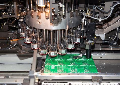
Innovations In Multilayer IMS PCB Manufacturing Techniques
In recent years, the field of electronics has witnessed significant advancements, particularly in the realm of printed circuit boards (PCBs). Among these innovations, multilayer Insulated Metal Substrate (IMS) PCBs have emerged as a pivotal development, offering enhanced thermal management and electrical performance. As electronic devices become increasingly compact and powerful, the demand for efficient heat dissipation and reliable performance has driven the evolution of multilayer IMS PCB manufacturing techniques.
To begin with, the fundamental advantage of IMS PCBs lies in their ability to effectively manage heat.
Traditional PCBs often struggle with heat dissipation, which can lead to reduced performance and potential failure of electronic components. In contrast, IMS PCBs incorporate a metal substrate, typically aluminum or copper, which acts as a heat sink. This substrate is layered with dielectric materials and copper circuits, allowing for superior thermal conductivity. As a result, multilayer IMS PCBs are particularly well-suited for high-power applications, such as LED lighting, automotive electronics, and power supplies.
Transitioning to the manufacturing techniques, one of the key innovations in multilayer IMS PCB production is the use of advanced materials.
Manufacturers are increasingly employing high-performance dielectric materials that offer improved thermal conductivity and electrical insulation. These materials are crucial in maintaining the integrity of the PCB while ensuring efficient heat transfer. Additionally, the development of thinner dielectric layers has enabled the production of more compact and lightweight PCBs, which are essential for modern electronic devices.
Moreover, advancements in fabrication processes have played a significant role in enhancing the quality and performance of multilayer IMS PCBs.
Techniques such as laser drilling and precision etching have allowed for the creation of intricate circuit patterns with high accuracy. These processes not only improve the electrical performance of the PCBs but also enable the integration of more complex circuitry within a smaller footprint. Furthermore, the adoption of automated manufacturing systems has increased production efficiency and consistency, reducing the likelihood of defects and ensuring high-quality output.
In addition to material and process innovations, the design of multilayer IMS PCBs has also evolved to meet the demands of contemporary applications.
Engineers are now able to design PCBs with multiple layers of circuitry, each serving a specific function. This multilayer approach allows for greater design flexibility and the integration of diverse functionalities within a single board. For instance, power and signal layers can be separated to minimize interference, while thermal layers can be strategically placed to optimize heat dissipation.
As we look to the future, the continued development of multilayer IMS PCB manufacturing techniques is expected to drive further advancements in electronic device performance.
The integration of emerging technologies, such as 5G and the Internet of Things (IoT), will likely necessitate even more sophisticated PCB designs and manufacturing processes. Consequently, ongoing research and innovation in materials, fabrication techniques, and design methodologies will be essential to meet these evolving requirements.
In conclusion, the innovations in multilayer IMS PCB manufacturing techniques have significantly enhanced the capabilities of electronic devices by improving thermal management and electrical performance. Through the use of advanced materials, precise fabrication processes, and innovative design strategies, manufacturers are able to produce high-quality PCBs that meet the demands of modern applications. As technology continues to advance, the role of multilayer IMS PCBs in the electronics industry is poised to become even more critical, driving further innovation and enabling the development of increasingly powerful and efficient electronic devices.