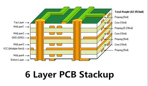
Exploring the Benefits of a 6 Layer PCB Prototype Design
Key Takeaways
When considering 6 layer PCB prototypes, it’s essential to recognize how they can significantly impact your projects and overall pcb manufacturing process. Utilizing a multi-layer design allows for a more compact and efficient layout, which can be particularly beneficial in devices with limited space. As you explore the advantages, keep in mind that pcb manufacturing companies often highlight the increased performance resilience that 6 layer PCBs provide, especially in high-frequency applications. Moreover, choosing this type of design can lead to a notable reduction in electromagnetic interference, making them an excellent option for maintaining signal integrity.
It’s also crucial to consider the investment aspect, as the pcb manufacturing cost may vary based on the complexity of your board and the specific needs of your project. However, this investment can be justified by the long-term benefits and reliability offered, particularly when dealing with intricate circuit designs. In engaging with pcb manufacturing business, you may find that opting for a 6 layer PCB prototype not only enhances the functionality of your product but also positions you favorably against competitors who may rely on simpler designs. Ultimately, embracing these multi-layer technologies could lead to meaningful advancements in your electronic endeavors.
Introduction to 6 Layer PCB Prototypes
When venturing into the realm of PCB manufacturing, one encounters various designs, among which the 6 layer PCB prototype stands out as a formidable choice. This advanced design allows you to optimize space and integrate more complex circuitry than traditional, simpler boards. Through 6 layer PCB designs, you can enhance your product’s performance significantly, making them suitable for demanding applications in industries like telecommunications, automotive, and consumer electronics. Moreover, working with PCB manufacturing companies that specialize in multi-layer designs can help manage costs while ensuring high-quality standards are met.
Understanding the intricate relationship between layer count and functionality is essential. The numerous layers contribute to superior signal integrity and minimize physical space consumption, all while maintaining a low PCB manufacturing cost. Such efficiency often translates into a competitive edge for your projects in the PCB manufacturing business.
“Investing in quality PCB prototypes is crucial for long-term success in electronics.”
By choosing a 6 layer design, you position yourself strategically in the market, ready to take on more sophisticated electronic challenges while adhering to best practices for effective design. This ensures that your final product not only meets but surpasses industry standards.
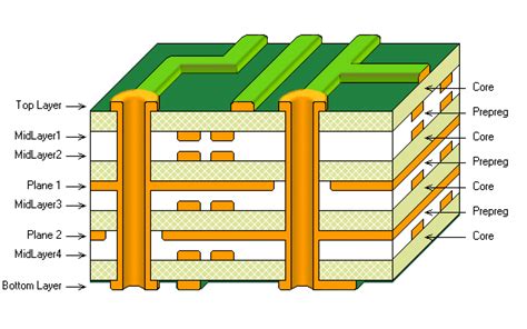
Key Advantages of Using a 6 Layer PCB Design
When considering the optimal approach for your electronic projects, utilizing a 6 layer PCB design offers numerous advantages that can significantly enhance your circuit’s functionality and efficiency. One of the most notable benefits is the improved performance achieved through better signal integrity and reduced crosstalk. With multiple layers, you can arrange sensitive components away from noisy signals, which leads to a cleaner performance in demanding applications. Furthermore, you gain the ability to support intricate circuitry setups that would be unattainable with simpler designs.
The flexibility provided by a 6 layer PCB enables more compact layouts, which is particularly beneficial for space-constrained devices. This capability allows you to include complex interconnections while maintaining the required separation for high-frequency applications—directly impacting your pcb manufacturing cost by minimizing material waste and optimizing space usage. Additionally, with advancements in technology, many pcb manufacturing companies now offer competitive pricing for advanced multilayer designs. This means you can invest in quality without exceeding your budget constraints.
Moreover, partnering with reputable pcb manufacturing companies ensures that your design adheres to industry standards while benefiting from state-of-the-art technology and techniques. Implementing a robust design that takes into account best practices during PCB layout not only elevates performance but also enhances reliability—a critical aspect for any pcb manufacturing business aiming to deliver quality products. Thus, adopting a multi-layer approach not only benefits your project but also positions you favorably in an increasingly competitive market.
| Feature | Standard PCB | 6 Layer PCB |
|---|---|---|
| Space Efficiency | Low | High |
| Signal Integrity | Moderate | High |
| Crosstalk Reduction | Limited | Significant |
| Manufacturing Cost | Low | Moderate (Varies) |
In summary, leveraging a 6 layer PCB design allows for optimized layouts while addressing complex electrical needs effectively—hallmarks that significantly contribute to innovative electronic solutions in today’s fast-evolving technological landscape.
Performance Enhancement Through Multi-Layer PCBs
When you consider the performance enhancement provided by a 6 layer PCB prototype, it’s crucial to understand how multi-layer designs can significantly optimize your projects. These sophisticated circuit boards offer a compact solution, allowing you to integrate more components without taking up excessive space. This density gives rise to improved performance, as it facilitates shorter traces, thus reducing signal delay and enhancing speed. In addition, by strategically layering the PCB manufacturing process, you can manage power distribution more effectively, which is vital in high-frequency applications.
As you explore partnerships with reputable pcb manufacturing companies, you will find that a 6 layer design not only supports your circuit’s performance but also minimizes the overall pcb manufacturing cost through efficient use of materials and space. This means that designing with multi-layer boards can lead to long-term savings in both production and functionality. Additionally, the intricate routing capabilities that come with this technology allow you to create complex circuitry without compromising signal integrity or introducing unnecessary noise.
In today’s competitive landscape of the pcb manufacturing business, adopting multi-layer PCBs becomes a strategic advantage. By enhancing performance while ensuring reliability and functionality, your products can stand out in an increasingly crowded market. You’ll gain not just better performance metrics but also a pathway to innovate and push the boundaries of what your electronic devices can achieve.
Noise Reduction in Complex Circuitry Applications
When dealing with complex circuitry, one of the paramount challenges is managing electromagnetic interference (EMI) and signal degradation. A 6 layer PCB prototype design significantly mitigates these issues through its enhanced routing capabilities and layer separation, thus preventing noise from contaminating sensitive signals. By effectively optimizing the pcb manufacturing process, you can achieve superior isolation between layers, allowing high-frequency signals to travel without interference. This is particularly crucial in applications that require precision, such as in telecommunications or advanced audio systems.
Investing in a 6 layer PCB prototype not only aids in reducing noise but also supports intricate routing strategies, which are essential for modern electronic devices. Additionally, collaborating with reputable pcb manufacturing companies helps ensure that your design is executed with the highest quality standards while managing the pcb manufacturing cost effectively. As you explore the landscape of PCB designs, understanding how these factors interplay will enhance your ability to deliver reliable and efficient circuits tailored to your project’s specifications. Whether you are starting a new pcb manufacturing business or upgrading your existing capabilities, embracing mult-layer designs can set you apart in a competitive market.
Best Practices for Designing 6 Layer PCBs
When venturing into 6 layer PCB design, adhering to best practices can significantly enhance your project’s success. Begin by thoroughly understanding the pcb manufacturing process, ensuring your designs are optimized for efficiency and cost-effectiveness. Select a reputable pcb manufacturing company that specializes in multi-layer boards, as their expertise can provide invaluable insights into material selections and fabrication methods.
During the design phase, prioritize the integrity of your signals by implementing proper routing techniques. This includes maintaining consistent width for traces and using vias wisely to minimize signal loss and crosstalk. You should also consider the pcb manufacturing cost; therefore, it’s wise to balance complexity with manufacturability. For example, when laying out your board, keep in mind that excessive layers can lead to increased costs—hence it’s crucial to illustrate only essential layers.
Additionally, effective thermal management is paramount in complex circuitry applications. Utilize ground planes and power planes strategically to improve thermal performance and reduce electromagnetic interference (EMI). By doing so, you not only comply with industry standards but also enhance the overall functionality of your circuit.
Lastly, confirm that your final design is thoroughly tested before production begins to avoid any potentially costly errors during the pcb manufacturing business process. By following these best practices, you ensure a high-quality prototype that meets both performance standards and budget considerations, paving the way for successful advancements in your projects.
Real-World Applications of 6 Layer PCBs
In today’s rapidly evolving technological landscape, the utilization of 6 layer PCBs has become integral across various industries. Your application might find its ideal match in sectors such as telecommunications, where high-speed data transfer demands enhanced performance and minimal signal degradation. In the automotive industry, 6 layer PCB prototypes are pivotal for complex systems like advanced driver-assistance systems (ADAS), which require reliable performance and durability under harsh conditions. Additionally, in medical devices, pcb manufacturing ensures precision and consistency—critical factors when dealing with life-saving equipment. As you explore options among pcb manufacturing companies, consider how incorporating multi-layer designs can lead to innovation within your products. The pcb manufacturing cost, while generally higher than simpler designs, is offset by the benefits gained in performance and reliability—making it a worthwhile investment for businesses that strive for excellence. Moreover, as technology advances, industries like IoT (Internet of Things) are leveraging these prototypes for their hectic demands on connectivity and power efficiency. By embracing the potential of 6 layer PCBs, you can position your product at the forefront of your industry, ensuring it meets future challenges effectively while capitalizing on emerging opportunities in the pcb manufacturing business realm.
Future Trends in PCB Design and Manufacturing
As technology continues to evolve, the landscape of PCB manufacturing is set to undergo significant changes. One of the most notable trends is the increasing demand for 6 layer PCB prototypes, which allow for more complex designs and improved functionality. As you engage with pcb manufacturing companies, expect to see innovations aimed at reducing the overall pcb manufacturing cost while enhancing performance. The transition toward automation and advanced manufacturing techniques is likely to streamline production processes, making fast turnarounds more accessible for businesses of all sizes. With sustainability becoming a focal point in modern electronics, many pcb manufacturing businesses are exploring eco-friendly materials and processes that minimize waste. By keeping an eye on these emerging trends, you can ensure that your designs are not only cutting-edge but also align with the industry’s future direction. This proactive approach can lead to greater efficiency and competitiveness in your projects involving multi-layer PCBs in various applications.
Conclusion: Embracing Innovation with Dual Sided Circuit Boards
In today’s rapidly evolving electronics landscape, the adoption of 6 layer PCB prototypes has become increasingly prevalent among PCB manufacturing companies. Such designs allow you to harness improved signal integrity while maintaining a compact footprint in your projects. Particularly in areas requiring intricate circuitry and diverse functionality, a well-executed 6 layer PCB design can significantly streamline the manufacturing process and enhance overall product reliability. As you consider the PCB manufacturing cost, it’s essential to recognize that investing in a multi-layer structure often yields long-term benefits, such as reduced electromagnetic interference and optimized thermal management. This shift toward advanced design techniques empowers PCB manufacturing businesses to innovate continually, ensuring that their products meet the demands of modern applications while maintaining competitiveness in the marketplace. Embracing these innovations not only enhances your projects but also positions you at the forefront of technological advancement in electronics.
Conclusion: Embracing Innovation with Dual Sided Circuit Boards
In today’s rapidly evolving technological landscape, 6 layer PCB prototypes stand out as a testament to innovation and efficiency. By utilizing a 6 layer PCB design, you can significantly enhance the performance and reliability of your electronic devices. The advancement in PCB manufacturing processes has enabled companies to create prototypes that not only support complex circuitry but also minimize potential noise interference, which is crucial for sensitive applications. As you explore options, consider how PCB manufacturing companies focus on quality, ensuring that your prototypes meet stringent standards while managing the overall PCB manufacturing cost effectively. This approach not only elevates the performance of your product but also strengthens its market viability. As you venture into the PCB manufacturing business, leveraging these multi-layer designs can give you a competitive edge, allowing you to cater to modern demands for sophisticated and efficient electronic solutions. Embracing these innovations positions you to meet future challenges head-on while maximizing the potential of layered circuit designs in your projects.
FAQs
What is a 6 layer PCB prototype?
A 6 layer PCB prototype refers to a printed circuit board that consists of six layers, allowing for complex circuit arrangements and improved functionality.
How does a 6 layer PCB help in reducing noise?
Utilizing a 6 layer PCB helps in managing and reducing electromagnetic interference (EMI) by providing better ground planes and signal routing, which ensures that noise from various components does not affect the overall performance.
What are the typical costs associated with PCB manufacturing?
The PCB manufacturing cost can vary based on several factors including material choice, design complexity, and order volume. Generally, a prototype may incur higher costs due to lower production runs but becomes more economical with larger batch sizes.
What should I consider when selecting PCB manufacturing companies?
When choosing PCB manufacturing companies, consider factors such as reputation, technology capabilities, production speed, and customer support to ensure that they meet your project’s requirements.
How can I ensure the best results from my PCB manufacturing business?
To achieve optimal results from your PCB manufacturing business, it’s crucial to invest in quality design software, maintain clear communication with manufacturers, and implement thorough testing protocols throughout the prototyping phase.