Metal clad pcb specifications
Understanding The Basics Of Metal Clad PCB Specifications
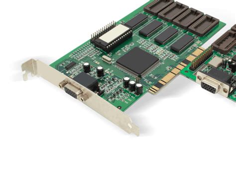
Metal Clad Printed Circuit Boards (PCBs) are a specialized type of PCB that incorporate a metal layer as part of their construction. This metal layer, typically made from aluminum or copper, serves as a heat sink to dissipate heat away from the components mounted on the board. Understanding the specifications of metal clad PCBs is crucial for engineers and designers who aim to optimize the thermal management of electronic devices. These specifications not only influence the performance and reliability of the final product but also determine the suitability of the PCB for specific applications.
To begin with, the choice of metal in metal clad PCBs is a fundamental specification.
Aluminum is commonly used due to its excellent thermal conductivity and cost-effectiveness. It is lightweight and provides a good balance between performance and price, making it suitable for a wide range of applications, including LED lighting and power electronics. Copper, on the other hand, offers superior thermal and electrical conductivity, which is beneficial for high-performance applications. However, it is more expensive and heavier than aluminum, which can be a limiting factor in certain designs.
Another critical specification is the thickness of the metal layer.
The thickness directly affects the PCB’s ability to dissipate heat. A thicker metal layer can handle more heat, which is advantageous for high-power applications. However, increasing the thickness also adds to the weight and cost of the PCB. Therefore, designers must carefully consider the trade-offs between thermal performance, weight, and cost when selecting the appropriate metal thickness for their application.
The dielectric layer, which separates the metal layer from the circuit layer, is another important specification.
This layer must have high thermal conductivity to efficiently transfer heat from the circuit layer to the metal layer. Additionally, it should possess good electrical insulation properties to prevent short circuits. The choice of dielectric material and its thickness can significantly impact the thermal performance and electrical reliability of the PCB.
Furthermore, the circuit layer specifications, including the copper thickness and trace width, play a vital role in the overall performance of metal clad PCBs.
The copper thickness must be sufficient to handle the current load without excessive heating, while the trace width should be optimized to minimize resistance and voltage drop. These factors are particularly important in high-current applications, where efficient power distribution is critical.
In addition to these material and dimensional specifications, the surface finish of metal clad PCBs is also a key consideration.
The surface finish protects the copper traces from oxidation and ensures good solderability. Common finishes include HASL (Hot Air Solder Leveling), ENIG (Electroless Nickel Immersion Gold), and OSP (Organic Solderability Preservative). Each finish has its advantages and limitations, and the choice depends on factors such as cost, environmental considerations, and the specific requirements of the application.
In conclusion, understanding the specifications of metal clad PCBs is essential for designing efficient and reliable electronic devices. By carefully selecting the appropriate metal type, thickness, dielectric material, circuit layer specifications, and surface finish, designers can optimize the thermal management and electrical performance of their PCBs. As electronic devices continue to evolve, the demand for effective thermal solutions will only increase, making metal clad PCBs an indispensable component in the electronics industry.
Key Material Considerations In Metal Clad PCB Design
In the realm of electronic design, metal clad printed circuit boards (PCBs) have emerged as a pivotal component, particularly in applications demanding efficient heat dissipation. These PCBs are distinguished by their unique construction, which incorporates a metal substrate, typically aluminum or copper, to enhance thermal management. As designers embark on the journey of metal clad PCB design, understanding the key material considerations becomes imperative to ensure optimal performance and reliability.
To begin with, the choice of metal substrate is a critical decision that influences the thermal and mechanical properties of the PCB.
Aluminum is often favored for its excellent thermal conductivity and lightweight nature, making it suitable for applications where weight is a concern. Conversely, copper, while heavier, offers superior thermal conductivity, which can be advantageous in high-power applications where heat dissipation is paramount. The selection between these metals hinges on the specific requirements of the application, balancing factors such as thermal performance, weight, and cost.
In addition to the metal substrate, the dielectric layer plays a crucial role in the overall performance of metal clad PCBs.
This layer, typically composed of a thermally conductive but electrically insulating material, serves as the interface between the metal substrate and the copper circuitry. The thermal conductivity of the dielectric material is a key parameter, as it directly impacts the board’s ability to transfer heat away from critical components. Materials with higher thermal conductivity are preferred, as they facilitate more efficient heat dissipation, thereby enhancing the reliability and longevity of the electronic device.
Moreover, the thickness of the dielectric layer is another important consideration.
A thinner dielectric layer can improve thermal performance by reducing the thermal resistance between the heat-generating components and the metal substrate. However, it is essential to ensure that the dielectric layer is sufficiently thick to provide adequate electrical insulation and mechanical support. Striking the right balance between thermal performance and electrical insulation is crucial in the design of metal clad PCBs.
Transitioning to the copper circuitry, the thickness of the copper layer is a determinant of the board’s current-carrying capacity.
Thicker copper layers can handle higher currents, which is beneficial in power electronics applications. However, increased copper thickness can also lead to higher costs and potential challenges in the manufacturing process. Therefore, designers must carefully evaluate the current requirements of their application to determine the appropriate copper thickness.
Furthermore, surface finish options for metal clad PCBs are an essential consideration, as they impact both the manufacturability and performance of the board.
Common finishes include HASL (Hot Air Solder Leveling), ENIG (Electroless Nickel Immersion Gold), and OSP (Organic Solderability Preservative). Each finish offers distinct advantages and trade-offs in terms of solderability, corrosion resistance, and cost. Selecting the appropriate surface finish is contingent upon the specific environmental and operational conditions the PCB will encounter.
In conclusion, the design of metal clad PCBs necessitates a comprehensive understanding of various material considerations, including the choice of metal substrate, dielectric properties, copper thickness, and surface finish. By meticulously evaluating these factors, designers can optimize the thermal management capabilities of their PCBs, ensuring robust performance in demanding applications. As technology continues to advance, the role of metal clad PCBs in facilitating efficient heat dissipation will undoubtedly become increasingly significant, underscoring the importance of informed material selection in the design process.
Thermal Management And Metal Clad PCB Specifications
Metal clad printed circuit boards (PCBs) have become increasingly significant in the realm of electronics, particularly due to their superior thermal management capabilities. As electronic devices continue to shrink in size while simultaneously increasing in power, the need for efficient heat dissipation has never been more critical. Metal clad PCBs, often referred to as metal core PCBs, are designed to address this very challenge by incorporating a metal layer that aids in the effective management of heat.
To understand the specifications of metal clad PCBs, it is essential to first consider their structure.
Typically, these PCBs consist of a metal base, a dielectric layer, and a copper circuit layer. The metal base, often made of aluminum or copper, serves as the primary heat dissipation medium. Aluminum is favored for its lightweight and cost-effectiveness, while copper is chosen for its superior thermal conductivity. The dielectric layer, which is thermally conductive yet electrically insulating, plays a crucial role in transferring heat from the circuit layer to the metal base. This configuration ensures that heat generated by electronic components is efficiently spread across the board and dissipated, thereby enhancing the performance and longevity of the device.
In terms of specifications, the thickness of the metal base is a critical factor.
It typically ranges from 0.5mm to 3mm, depending on the thermal requirements of the application. A thicker metal base can handle higher thermal loads, making it suitable for high-power applications. Conversely, a thinner base is used in applications where weight and space are constraints. The choice of metal also influences the thermal performance; for instance, copper, with its higher thermal conductivity, is preferred in applications demanding rapid heat dissipation.
The dielectric layer’s thermal conductivity is another vital specification.
It is usually measured in watts per meter-kelvin (W/mK), with values ranging from 1 W/mK to 4 W/mK or higher. A higher thermal conductivity indicates better heat transfer capabilities, which is crucial for maintaining optimal operating temperatures of electronic components. Additionally, the dielectric layer’s thickness, typically between 50µm and 200µm, affects the overall thermal resistance of the PCB. A thinner dielectric layer generally results in lower thermal resistance, facilitating more efficient heat transfer.
Furthermore, the copper circuit layer’s thickness, often specified in ounces per square foot, impacts both the electrical and thermal performance of the PCB.
Common thicknesses range from 1 oz/ft² to 3 oz/ft², with thicker copper layers providing lower electrical resistance and better current-carrying capacity. This is particularly important in applications where high current levels are involved.
In conclusion, the specifications of metal clad PCBs are intricately linked to their thermal management capabilities. By carefully selecting the appropriate materials and dimensions for the metal base, dielectric layer, and copper circuit layer, manufacturers can tailor these PCBs to meet the specific thermal and electrical requirements of various applications. As the demand for compact, high-performance electronic devices continues to grow, the role of metal clad PCBs in ensuring efficient thermal management will undoubtedly become even more pivotal. Through their innovative design and material composition, these PCBs offer a robust solution to the ever-present challenge of heat dissipation in modern electronics.
Comparing Metal Clad PCB Specifications Across Different Applications
Metal clad printed circuit boards (PCBs) have become increasingly significant in various industries due to their unique ability to efficiently dissipate heat, thereby enhancing the performance and reliability of electronic devices. These PCBs are particularly favored in applications where thermal management is crucial, such as in LED lighting, power electronics, and automotive systems. As we delve into the specifications of metal clad PCBs across different applications, it is essential to understand the fundamental components and characteristics that define their performance.
At the core of metal clad PCBs is a metal substrate, typically aluminum or copper, which serves as the primary heat dissipation layer.
The choice of metal substrate is often dictated by the specific thermal and mechanical requirements of the application. For instance, aluminum is commonly used due to its excellent thermal conductivity and cost-effectiveness, making it suitable for LED lighting applications where efficient heat dissipation is paramount. On the other hand, copper, with its superior thermal and electrical conductivity, is preferred in high-performance power electronics where both heat management and electrical performance are critical.
In addition to the metal substrate, the dielectric layer plays a pivotal role in the overall performance of metal clad PCBs.
This layer, which electrically insulates the conductive copper circuitry from the metal base, must possess high thermal conductivity to facilitate effective heat transfer. The thickness and material composition of the dielectric layer can vary significantly depending on the application. For example, in automotive systems where reliability under extreme conditions is essential, a thicker dielectric layer with enhanced thermal properties may be employed to ensure durability and performance.
Furthermore, the copper circuitry layer, which forms the electrical pathways on the PCB, is another crucial specification to consider.
The thickness of this layer can influence both the electrical performance and the thermal management capabilities of the PCB. In applications such as power electronics, where high current carrying capacity is required, a thicker copper layer is often utilized to minimize resistive losses and improve heat dissipation. Conversely, in applications where space and weight are constraints, such as in portable electronic devices, a thinner copper layer may be preferred to achieve a more compact design.
Transitioning to the aspect of design flexibility, metal clad PCBs offer a range of customization options to meet the specific needs of different applications.
For instance, the layout and pattern of the copper circuitry can be tailored to optimize thermal paths and enhance heat dissipation. Additionally, surface finishes such as HASL (Hot Air Solder Leveling), ENIG (Electroless Nickel Immersion Gold), or OSP (Organic Solderability Preservatives) can be applied to improve solderability and protect against oxidation, further extending the lifespan of the PCB.
In conclusion, the specifications of metal clad PCBs are intricately linked to their intended applications, with each component playing a vital role in determining the overall performance and reliability of the final product. By carefully selecting the appropriate metal substrate, dielectric layer, and copper circuitry, manufacturers can tailor metal clad PCBs to meet the diverse demands of industries ranging from LED lighting to automotive systems. As technology continues to advance, the versatility and adaptability of metal clad PCBs will undoubtedly play a crucial role in shaping the future of electronic device design and manufacturing.