Manufacturing process of single sided pcb
Overview about the manufacturing Process of Single Sided pcb
The manufacturing process of single-sided printed circuit boards (PCBs) is a meticulous and intricate procedure that requires precision and attention to detail. Single-sided PCBs, characterized by having components on one side and a conductive layer on the other, are widely used in various electronic devices due to their simplicity and cost-effectiveness. Understanding the manufacturing process of these PCBs is essential for appreciating their role in the electronics industry.
The journey of creating a single-sided PCB begins with the selection of the base material, typically a fiberglass-reinforced epoxy laminate known as FR-4.
This material is chosen for its excellent insulating properties and mechanical strength. The laminate is coated with a thin layer of copper on one side, which will form the conductive pathways of the circuit. The thickness of the copper layer is carefully selected based on the current-carrying requirements of the final product.
Once the base material is prepared, the next step involves designing the circuit pattern.
This is achieved through a process called photolithography, where a photoresist material is applied to the copper surface. The photoresist is a light-sensitive substance that hardens when exposed to ultraviolet (UV) light. A photomask, which contains the desired circuit pattern, is placed over the photoresist-coated board. When exposed to UV light, the areas of the photoresist not covered by the mask harden, while the unexposed areas remain soft and can be washed away, revealing the copper beneath.
Following the development of the circuit pattern, the board undergoes an etching process.
In this stage, the board is submerged in a chemical solution, typically ferric chloride or ammonium persulfate, which dissolves the exposed copper areas, leaving behind the desired circuit pattern protected by the hardened photoresist. This step is crucial as it defines the electrical pathways that will connect the components on the PCB.
After etching, the remaining photoresist is removed, and the board is thoroughly cleaned to ensure no residues are left.
The next phase involves drilling holes for component leads and mounting points. Precision drilling machines equipped with tiny drill bits are used to create these holes, which are essential for the assembly of electronic components onto the board.
Subsequently, the board undergoes a solder mask application.
The solder mask is a protective layer applied over the copper traces to prevent oxidation and accidental short circuits during soldering. It also provides a surface for the application of silkscreen, which is used to print component labels and other necessary markings on the board.
Finally, the single-sided PCB is subjected to a series of quality control tests to ensure its functionality and reliability.
These tests may include electrical testing to verify the integrity of the circuit connections and visual inspections to check for any physical defects. Once the board passes these tests, it is ready for assembly, where electronic components are soldered onto the board to create a functional electronic device.
In conclusion, the manufacturing process of single-sided PCBs involves a series of carefully controlled steps, each contributing to the creation of a reliable and efficient circuit board. From material selection to final testing, each phase is crucial in ensuring that the end product meets the required standards and functions as intended in its application.
Key Steps In Single Sided PCB Production
The manufacturing process of single-sided printed circuit boards (PCBs) is a meticulous and intricate procedure that involves several key steps, each crucial to ensuring the final product’s functionality and reliability. Single-sided PCBs, characterized by having components on only one side of the board, are widely used in various electronic devices due to their simplicity and cost-effectiveness. Understanding the key steps in their production provides insight into the precision and expertise required in the field of electronics manufacturing.
Initially, the process begins with the selection of the base material, typically a fiberglass-reinforced epoxy laminate known as FR-4.
This material is chosen for its excellent insulating properties and mechanical strength. The laminate is coated with a thin layer of copper on one side, which will form the conductive pathways of the PCB. The thickness of the copper layer is carefully controlled to meet the specific requirements of the intended application.
Following the preparation of the base material, the next step involves designing the circuit pattern.
This is achieved through a process called photolithography. A photosensitive film, known as a photoresist, is applied to the copper surface. The circuit design is then transferred onto the photoresist using ultraviolet light. Areas exposed to the light become hardened, while unexposed areas remain soft and can be washed away, revealing the copper beneath.
Once the circuit pattern is established, the board undergoes an etching process.
In this step, the board is immersed in a chemical solution, typically ferric chloride or ammonium persulfate, which dissolves the unprotected copper, leaving behind only the desired circuit traces. This step requires precise control to ensure that the etching is uniform and that the circuit paths are not compromised.
Subsequently, the board is cleaned to remove any residual chemicals and photoresist,
preparing it for the next stage: drilling. Holes are drilled into the board to accommodate component leads and mounting hardware. The precision of this step is critical, as any misalignment can affect the board’s functionality. Advanced CNC machines are often employed to achieve the necessary accuracy and speed.
Following drilling, the board undergoes a solder mask application.
The solder mask is a protective layer that covers the entire board except for the areas where components will be soldered. This layer prevents solder bridges from forming between closely spaced circuit paths and protects the copper traces from environmental damage.
The final step in the manufacturing process is the application of a silkscreen layer.
This layer provides labels and markings on the board, indicating component placement and other important information. The silkscreen is typically applied using a screen-printing process, ensuring that the markings are clear and durable.
In conclusion, the production of single-sided PCBs involves a series of carefully controlled steps, each contributing to the board’s overall quality and performance. From the selection of materials to the final application of the silkscreen, each phase requires precision and expertise. As technology continues to advance, the methods and materials used in PCB manufacturing are continually refined, ensuring that single-sided PCBs remain a vital component in the electronics industry.
Materials Used In Single Sided PCB Fabrication
In the realm of electronics, the manufacturing process of single-sided printed circuit boards (PCBs) is a fundamental aspect that underpins the functionality of countless devices. Central to this process is the selection and utilization of appropriate materials, which play a crucial role in determining the performance, reliability, and cost-effectiveness of the final product. Understanding the materials used in single-sided PCB fabrication is essential for appreciating the intricacies involved in their production.
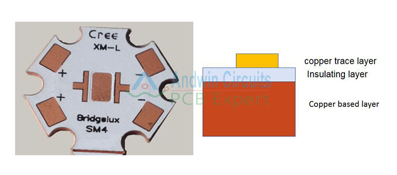
To begin with, the base material, or substrate, forms the foundation of a single-sided PCB.
Typically, this substrate is composed of a dielectric material, with FR-4 being the most commonly used. FR-4 is a composite material made from woven fiberglass cloth with an epoxy resin binder that is flame resistant. Its popularity stems from its excellent mechanical strength, thermal resistance, and electrical insulation properties, making it an ideal choice for a wide range of applications. However, for cost-sensitive projects, alternative materials such as phenolic or paper-based substrates may be employed, albeit with some trade-offs in performance.
On top of the substrate lies a thin layer of conductive material, usually copper, which is essential for forming the electrical pathways on the PCB.
Copper is favored due to its excellent electrical conductivity and relative ease of etching, which is a critical step in the PCB manufacturing process. The thickness of the copper layer can vary depending on the specific requirements of the application, with common thicknesses ranging from 1 oz/ft² to 3 oz/ft². This copper layer is initially applied to the entire surface of the substrate and is later selectively removed to create the desired circuit pattern.
In addition to the substrate and copper layer, a protective solder mask is applied to the PCB.
This layer serves multiple purposes: it insulates the copper traces to prevent short circuits, protects the copper from oxidation and environmental damage, and provides a surface for soldering components. The solder mask is typically made from a polymer-based material and is available in various colors, with green being the most prevalent due to its visibility and ease of inspection.
Furthermore, a silkscreen layer is often added to the PCB to provide important information such as component labels, part numbers, and logos.
This layer is applied using a non-conductive ink, which is usually white, although other colors can be used depending on the design requirements. The silkscreen aids in the assembly and maintenance of the PCB by providing clear visual guidance.
Finally, the choice of materials for single-sided PCB fabrication is not solely dictated by technical considerations.
Economic factors also play a significant role, as manufacturers must balance performance with cost-effectiveness to remain competitive. This often involves making strategic decisions about material selection based on the intended application and production volume.
In conclusion, the materials used in the fabrication of single-sided PCBs are integral to their functionality and performance. From the substrate and copper layer to the solder mask and silkscreen, each material is carefully chosen to meet specific technical and economic criteria. By understanding these materials and their roles, one gains a deeper appreciation for the complexity and precision involved in the manufacturing process of single-sided PCBs.
Common Challenges In Single Sided PCB Manufacturing
The manufacturing process of single-sided printed circuit boards (PCBs) is a complex endeavor that involves several intricate steps, each of which presents its own set of challenges. Understanding these challenges is crucial for manufacturers aiming to produce high-quality PCBs efficiently and cost-effectively. One of the primary challenges in single-sided PCB manufacturing is ensuring the precision of the etching process. Etching is a critical step where unwanted copper is removed to create the desired circuit pattern. However, achieving the exact pattern can be difficult due to variations in etching rates, which can be influenced by factors such as temperature, chemical concentration, and exposure time. Inconsistencies in these parameters can lead to over-etching or under-etching, resulting in defective circuits.
Moreover, the quality of the substrate material used in single-sided PCBs can significantly impact the manufacturing process
The substrate must possess excellent thermal and mechanical properties to withstand the various stages of production. However, selecting the appropriate substrate material can be challenging due to the wide range of options available, each with its own advantages and limitations. For instance, while FR-4 is a popular choice due to its good balance of cost and performance, it may not be suitable for applications requiring high thermal resistance. Consequently, manufacturers must carefully evaluate the specific requirements of the end application to choose the most suitable substrate.
Another challenge lies in the drilling process, which involves creating holes for component leads and vias.
Precision in drilling is paramount, as any deviation can lead to misalignment and connectivity issues. The use of advanced drilling machines with high accuracy is essential, yet even with such equipment, factors like drill bit wear and substrate thickness can affect the outcome. Regular maintenance of drilling equipment and careful monitoring of the process are necessary to mitigate these issues.
Furthermore, the solder mask application presents its own set of challenges.
The solder mask is a protective layer applied over the copper traces to prevent short circuits and corrosion. Achieving uniform coverage without defects such as bubbles or peeling is crucial for the reliability of the PCB. However, variations in the viscosity of the solder mask material, application pressure, and curing conditions can lead to inconsistencies. Manufacturers must ensure that the application process is tightly controlled and that the materials used are of high quality to avoid such defects.
In addition to these technical challenges, single-sided PCB manufacturing also faces logistical issues related to supply chain management.
The availability and cost of raw materials can fluctuate, impacting production schedules and overall costs. Manufacturers must establish robust supply chain strategies to ensure a steady flow of materials and minimize disruptions.
Finally, quality control is a pervasive challenge throughout the manufacturing process.
Each step must be meticulously monitored to detect and rectify defects early. Implementing comprehensive testing and inspection protocols, such as automated optical inspection (AOI) and electrical testing, is essential to ensure that the final product meets the required specifications and standards.
In conclusion, while the manufacturing process of single-sided PCBs is fraught with challenges, understanding and addressing these issues is vital for producing reliable and high-quality products. By focusing on precision, material selection, process control, and quality assurance, manufacturers can overcome these obstacles and achieve success in the competitive PCB market.