Manufacturing process of pcb board
Understanding The Basics Of PCB Manufacturing
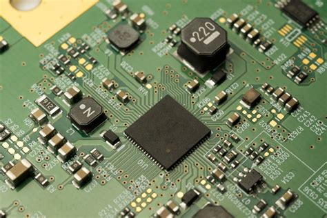
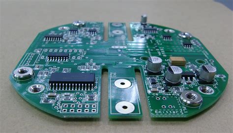
Printed Circuit Boards (PCBs) are the backbone of modern electronic devices, serving as the foundation upon which electronic components are mounted and interconnected. Understanding the basics of PCB manufacturing is essential for anyone involved in electronics design and production. The process begins with the design phase, where engineers use specialized software to create a schematic diagram and layout of the circuit. This design is then translated into a digital file format, typically Gerber files, which serve as the blueprint for the manufacturing process.
Once the design is finalized, the next step is to select the appropriate materials.
PCBs are typically made from a substrate material, such as fiberglass-reinforced epoxy resin, known as FR-4. This material provides the necessary mechanical support and electrical insulation. Copper is then laminated onto the substrate to form the conductive pathways. The thickness of the copper layer can vary depending on the specific requirements of the circuit, with common thicknesses being one ounce per square foot.
Following material selection, the manufacturing process moves to the fabrication stage.
This begins with the transfer of the circuit design onto the copper-clad substrate. A common method for this is photolithography, where a photosensitive film is applied to the copper surface. The film is then exposed to ultraviolet light through a mask that represents the circuit pattern. The exposed areas of the film harden, while the unexposed areas remain soft and are subsequently washed away, revealing the copper beneath.
The next step is etching, where the exposed copper is removed using a chemical solution, leaving behind only the desired circuit pattern.
This is a critical stage, as precision is paramount to ensure that the circuit functions correctly. After etching, the board undergoes a process called drilling, where holes are made for component leads and vias, which are used to connect different layers of the board.
Once drilling is complete, the board is plated with a thin layer of copper to ensure electrical connectivity through the holes.
This is followed by the application of a solder mask, which is a protective layer that prevents solder from bridging between conductive traces and causing short circuits. The solder mask also provides a surface for the application of silkscreen, which is used to print component labels and other important information on the board.
The final stages of PCB manufacturing involve testing and quality control.
Each board is subjected to electrical testing to verify that there are no open circuits or shorts. This is typically done using a flying probe tester or a bed of nails fixture. Any defects identified during testing are addressed before the boards are approved for assembly.
In conclusion, the manufacturing process of a PCB board is a complex and precise operation that requires careful attention to detail at every stage. From design and material selection to fabrication and testing, each step is crucial to ensure the final product meets the required specifications and functions as intended. Understanding these basics provides valuable insight into the intricate world of electronics manufacturing, highlighting the importance of precision and quality in producing reliable and efficient electronic devices.
Key Steps In The PCB Fabrication Process
The manufacturing process of a printed circuit board (PCB) is a complex and intricate procedure that involves several key steps, each crucial to ensuring the final product meets the required specifications and quality standards. Understanding these steps provides insight into how electronic devices are brought to life, as PCBs serve as the backbone of most electronic systems.
Initially, the process begins with the design phase, where engineers use specialized software to create a detailed blueprint of the PCB layout.
This design includes the placement of components, the routing of electrical connections, and the specification of layers. Once the design is finalized, it is converted into a format suitable for manufacturing, typically a Gerber file, which contains all the necessary information for the subsequent fabrication steps.
Following the design phase, the next step is the preparation of the substrate, which serves as the foundation of the PCB.
The substrate is usually made from a non-conductive material such as fiberglass, which is coated with a thin layer of copper on one or both sides. This copper layer will eventually form the conductive pathways that connect various components on the board. The substrate is cleaned and prepared to ensure that it is free from any contaminants that could affect the adhesion of the copper.
Subsequently, the process of transferring the circuit design onto the substrate begins.
This is typically achieved through a method known as photolithography. In this step, a photosensitive film, or photoresist, is applied to the copper-clad substrate. The board is then exposed to ultraviolet light through a mask that represents the circuit pattern. The areas of the photoresist exposed to the light harden, while the unexposed areas remain soft and can be washed away, revealing the underlying copper.
Once the circuit pattern is established, the next step involves etching away the unwanted copper.
This is done using a chemical solution that removes the exposed copper, leaving behind only the desired circuit traces protected by the hardened photoresist. After etching, the remaining photoresist is stripped away, revealing the copper traces that form the electrical pathways of the PCB.
The process then moves to drilling, where holes are created for component leads and vias, which are used to connect different layers of the board.
Precision drilling machines are employed to ensure accuracy and consistency in hole placement and size. Following drilling, the board undergoes a plating process, where a thin layer of copper is deposited into the holes and on the surface to enhance conductivity and provide a base for soldering components.
Subsequently, a solder mask is applied to the board to protect the copper traces from oxidation and to prevent solder bridges during component assembly.
The solder mask is typically a green epoxy layer that covers the entire board except for the pads where components will be soldered. Finally, a silkscreen layer is added, which provides labels and markings to assist in component placement and identification.
In conclusion, the PCB fabrication process is a meticulous sequence of steps that transforms a design into a functional electronic component. Each stage, from design to final finishing, plays a vital role in ensuring the reliability and performance of the PCB. Understanding these key steps highlights the precision and expertise required in the manufacturing of PCBs, which are essential to the operation of modern electronic devices.
Innovations In PCB Manufacturing Technology
The manufacturing process of printed circuit boards (PCBs) has undergone significant innovations over the years, driven by the relentless pursuit of efficiency, precision, and miniaturization. As the backbone of modern electronic devices, PCBs are integral to the functionality of everything from smartphones to industrial machinery. Consequently, advancements in PCB manufacturing technology are crucial to meeting the ever-evolving demands of the electronics industry.
One of the most notable innovations in PCB manufacturing is the adoption of advanced materials.
Traditionally, PCBs were made using fiberglass-reinforced epoxy laminate, known as FR-4. However, the need for higher performance and reliability has led to the exploration of alternative materials such as polyimide and ceramic substrates. These materials offer superior thermal stability and electrical performance, making them ideal for high-frequency and high-power applications. By utilizing these advanced materials, manufacturers can produce PCBs that are not only more robust but also capable of supporting the increasing complexity of modern electronic circuits.
In addition to material advancements, the manufacturing process itself has seen significant improvements.
Automation and precision machinery have revolutionized PCB fabrication, allowing for greater accuracy and consistency. Computer numerical control (CNC) machines, for instance, have replaced manual drilling and routing processes, significantly reducing human error and increasing production speed. Furthermore, the integration of laser technology in cutting and drilling processes has enabled manufacturers to achieve finer tolerances and more intricate designs, which are essential for the miniaturization of electronic components.
Another key innovation in PCB manufacturing is the development of advanced imaging and printing techniques.
Traditional photolithography, while still widely used, has been complemented by direct imaging technologies that utilize laser or inkjet systems to apply circuit patterns directly onto the substrate. This not only enhances precision but also reduces the number of steps involved in the process, thereby increasing efficiency. Moreover, these techniques allow for greater flexibility in design modifications, enabling rapid prototyping and customization to meet specific client requirements.
The rise of additive manufacturing, commonly known as 3D printing, has also made its mark on PCB production.
While still in its nascent stages, 3D printing offers the potential to revolutionize the industry by enabling the creation of complex, multi-layered PCBs in a single process. This technology allows for the integration of components directly into the board, reducing the need for separate assembly steps and potentially lowering production costs. As 3D printing technology continues to evolve, it is expected to play an increasingly significant role in PCB manufacturing.
Environmental considerations have also spurred innovations in PCB manufacturing.
The industry has made strides in reducing its ecological footprint by adopting more sustainable practices. For instance, the use of lead-free solder and the implementation of waste reduction strategies have become standard in many manufacturing facilities. Additionally, advancements in recycling technologies have enabled the recovery and reuse of valuable materials from discarded PCBs, contributing to a more circular economy.
In conclusion, the innovations in PCB manufacturing technology are a testament to the industry’s commitment to advancing electronic design and production. By embracing new materials, automation, advanced imaging techniques, and sustainable practices, manufacturers are not only enhancing the performance and reliability of PCBs but also paving the way for future technological breakthroughs. As the demand for more sophisticated electronic devices continues to grow, the ongoing evolution of PCB manufacturing will undoubtedly play a pivotal role in shaping the future of the electronics industry.
Quality Control Measures In PCB Production
In the intricate world of electronics, the manufacturing process of printed circuit boards (PCBs) is a critical component that demands precision and attention to detail. As the backbone of electronic devices, PCBs must adhere to stringent quality control measures to ensure their reliability and functionality. The quality control process in PCB production is multifaceted, encompassing various stages that collectively contribute to the production of high-quality boards.
Initially, the quality control process begins with the inspection of raw materials.
Ensuring that the materials used, such as copper-clad laminates and solder masks, meet industry standards is crucial. This preliminary step helps prevent defects that could arise from substandard materials. Once the materials are verified, the focus shifts to the design verification stage. Here, the PCB design is meticulously reviewed to ensure it aligns with the intended specifications and functionality. This stage often involves the use of advanced software tools that simulate the board’s performance, allowing engineers to identify and rectify potential issues before production begins.
As the manufacturing process progresses, the etching stage is another critical point where quality control measures are rigorously applied.
During etching, unwanted copper is removed to create the desired circuit patterns. Precision is paramount, as any deviation can lead to circuit failures. To mitigate this risk, manufacturers employ automated optical inspection (AOI) systems that scan the etched boards for defects such as over-etching or under-etching. These systems provide a high level of accuracy, ensuring that only boards meeting the exact specifications proceed to the next stage.
Subsequently, the drilling process, which involves creating holes for component leads and vias, is subject to stringent quality checks.
The accuracy of hole placement and size is vital for the proper functioning of the PCB. Advanced drilling machines equipped with laser guidance systems are often used to achieve the necessary precision. Post-drilling, the boards undergo another round of AOI to verify the integrity of the drilled holes.
The solder mask application is another crucial step where quality control is indispensable.
The solder mask serves as a protective layer, preventing solder bridges and short circuits. Ensuring its uniform application is essential, and this is achieved through automated systems that apply and cure the mask under controlled conditions. Any inconsistencies in the solder mask can lead to significant issues during the assembly process, making this a critical quality checkpoint.
Finally, the electrical testing phase serves as the ultimate quality control measure.
This involves subjecting the PCB to a series of tests to verify its electrical integrity and functionality. Techniques such as in-circuit testing (ICT) and flying probe testing are employed to detect open circuits, short circuits, and other potential defects. These tests are crucial in ensuring that the final product meets the required performance standards.
In conclusion, the quality control measures in PCB production are comprehensive and meticulously implemented at every stage of the manufacturing process. From the inspection of raw materials to the final electrical testing, each step is designed to ensure that the PCBs produced are of the highest quality. By adhering to these rigorous standards, manufacturers can deliver reliable and efficient PCBs that meet the demands of modern electronic applications.