Learn high speed pcb design
Understanding Signal Integrity in High-Speed PCB Design
In the realm of high-speed printed circuit board (PCB) design, understanding signal integrity is paramount to ensuring optimal performance and reliability of electronic systems. As technology advances, the demand for faster data transmission rates has increased, necessitating a deeper comprehension of the factors that influence signal integrity. At its core, signal integrity refers to the quality and reliability of electrical signals as they travel through a PCB. It encompasses various phenomena such as signal reflection, crosstalk, and electromagnetic interference, all of which can degrade the performance of high-speed circuits.
To begin with, signal reflection occurs when a signal encounters an impedance mismatch along its transmission path.
This mismatch can cause a portion of the signal to be reflected back towards the source, leading to potential data corruption. To mitigate this issue, designers must carefully match the impedance of transmission lines with the source and load. This involves selecting appropriate trace widths, dielectric materials, and ensuring proper termination techniques are employed. By doing so, the risk of signal reflection is minimized, thereby preserving signal integrity.
In addition to signal reflection, crosstalk is another critical factor that can adversely affect signal integrity in high-speed PCB design.
Crosstalk arises when a signal in one trace induces an unwanted signal in an adjacent trace, primarily due to capacitive or inductive coupling. This can lead to errors in data transmission, particularly in densely packed PCBs where traces are in close proximity. To address crosstalk, designers can implement strategies such as increasing the spacing between traces, using differential signaling, and incorporating ground planes to provide a return path for signals. These measures help to isolate signals and reduce the likelihood of crosstalk, thereby enhancing signal integrity.
Moreover, electromagnetic interference (EMI) poses a significant challenge in maintaining signal integrity.
EMI can originate from both internal and external sources, potentially disrupting the operation of high-speed circuits. To combat EMI, designers can employ shielding techniques, such as using ground planes and metal enclosures, to contain and isolate electromagnetic fields. Additionally, careful routing of traces and strategic placement of components can minimize the susceptibility of the PCB to EMI. By addressing EMI concerns, designers can ensure that signals remain intact and free from external disturbances.
Furthermore, the choice of materials and components plays a crucial role in preserving signal integrity.
High-speed PCBs often require materials with low dielectric constants and low loss tangents to minimize signal attenuation. Selecting components with appropriate bandwidth and rise time specifications is also essential to prevent signal distortion. By making informed decisions regarding materials and components, designers can optimize the performance of high-speed circuits and maintain signal integrity.
In conclusion, understanding signal integrity is a fundamental aspect of high-speed PCB design. By addressing issues such as signal reflection, crosstalk, and electromagnetic interference, designers can ensure the reliable transmission of signals in high-speed circuits. Through careful impedance matching, strategic trace routing, and the use of appropriate materials and components, signal integrity can be preserved, leading to enhanced performance and reliability of electronic systems. As technology continues to evolve, the importance of signal integrity in high-speed PCB design will only grow, underscoring the need for designers to stay informed and adept in this critical area.
Essential Tools and Software for High-Speed PCB Design
In the realm of high-speed PCB (Printed Circuit Board) design, the selection of appropriate tools and software is paramount to achieving optimal performance and reliability. As electronic devices become increasingly complex, the demand for high-speed circuits has surged, necessitating a meticulous approach to PCB design. To navigate this intricate process, designers must equip themselves with a suite of essential tools and software that facilitate precision, efficiency, and innovation.
Foremost among these tools is PCB design software, which serves as the foundation for creating and simulating circuit layouts.
Industry-leading software such as Altium Designer, Cadence Allegro, and Mentor Graphics PADS offer comprehensive features tailored to high-speed design requirements. These platforms provide advanced routing capabilities, signal integrity analysis, and design rule checks, enabling designers to visualize and optimize their circuits effectively. By leveraging these tools, designers can ensure that their layouts adhere to the stringent demands of high-speed applications, minimizing the risk of signal degradation and electromagnetic interference.
In addition to design software, simulation tools play a crucial role in high-speed PCB design.
Signal integrity simulators, such as Ansys HFSS and Keysight ADS, allow designers to model and analyze the behavior of high-frequency signals within their circuits. These tools enable the identification of potential issues such as crosstalk, reflection, and impedance mismatches, which can adversely affect signal quality. By simulating these scenarios, designers can make informed decisions regarding trace routing, layer stack-up, and component placement, ultimately enhancing the performance and reliability of the final product.
Moreover, electromagnetic compatibility (EMC) analysis tools are indispensable in high-speed PCB design.
As electronic devices operate at higher frequencies, they become more susceptible to electromagnetic interference (EMI), which can compromise functionality. Tools like CST Studio Suite and EMPro provide designers with the ability to assess and mitigate EMI risks by simulating electromagnetic fields and evaluating the impact of design choices on EMC performance. Through these analyses, designers can implement strategies such as shielding, filtering, and grounding to ensure compliance with regulatory standards and enhance the overall robustness of their designs.
Transitioning from simulation to physical implementation, fabrication tools are essential for translating digital designs into tangible PCBs.
Gerber file generators, such as CAM350 and ViewMate, facilitate the conversion of design files into a format suitable for manufacturing. These tools ensure that the intricate details of high-speed designs are accurately represented in the final product, minimizing the likelihood of errors during fabrication. Additionally, design for manufacturability (DFM) tools help designers optimize their layouts for efficient production, reducing costs and lead times.
Finally, collaboration and version control tools are vital for managing the complexities of high-speed PCB design projects.
Platforms like Git and SVN enable teams to collaborate seamlessly, track changes, and maintain a comprehensive history of design iterations. This collaborative approach fosters innovation and ensures that all stakeholders are aligned throughout the design process.
In conclusion, the successful execution of high-speed PCB design hinges on the strategic use of specialized tools and software. By integrating design, simulation, fabrication, and collaboration tools into their workflow, designers can navigate the challenges of high-speed circuits with confidence and precision. As technology continues to evolve, staying abreast of advancements in these tools will be essential for designers seeking to push the boundaries of what is possible in high-speed PCB design.
Best Practices for Layer Stackup in High-Speed PCB Design
In the realm of high-speed PCB design, the layer stackup plays a pivotal role in ensuring signal integrity, minimizing electromagnetic interference, and optimizing overall performance. As electronic devices become increasingly complex, the demand for efficient and reliable PCB designs has never been greater. Understanding the best practices for layer stackup is essential for engineers and designers aiming to meet these demands.
To begin with, the selection of the number of layers in a PCB is a critical decision that impacts both the functionality and cost of the design.
A well-considered layer stackup can significantly enhance signal integrity by providing dedicated layers for power, ground, and signal routing. Typically, high-speed designs benefit from a multilayer approach, often comprising four or more layers. This configuration allows for the separation of signal and power planes, reducing the potential for crosstalk and electromagnetic interference.
Transitioning to the arrangement of these layers, it is advisable to position power and ground planes adjacent to each other.
This proximity creates a low-inductance path, which is crucial for maintaining stable power delivery and minimizing noise. Furthermore, placing signal layers between power and ground planes can effectively shield them from external interference, thereby preserving signal quality. This sandwich-like structure is often referred to as a “stripline” configuration and is favored for its ability to maintain consistent impedance.
Moreover, the concept of controlled impedance is integral to high-speed PCB design.
As signal frequencies increase, maintaining a consistent impedance becomes paramount to prevent signal reflections and losses. To achieve this, designers must carefully calculate the trace width, spacing, and dielectric thickness between layers. Utilizing simulation tools can aid in predicting and optimizing these parameters, ensuring that the PCB meets the desired impedance specifications.
In addition to impedance control, the choice of materials for the PCB substrate is another crucial consideration.
High-speed designs often require materials with low dielectric constants and low loss tangents to minimize signal attenuation. FR-4 is a common choice for many applications; however, for extremely high-speed designs, alternative materials such as Rogers or Teflon may be more suitable due to their superior electrical properties.
Transitioning to the topic of thermal management, it is important to recognize that high-speed PCBs can generate significant heat.
Effective thermal management is essential to prevent overheating and ensure reliable operation. Incorporating thermal vias and heat sinks, as well as selecting materials with good thermal conductivity, can help dissipate heat efficiently. Additionally, careful placement of components and consideration of airflow can further enhance thermal performance.
Finally, it is essential to consider the manufacturability of the PCB design.
While advanced layer stackups can offer significant performance benefits, they can also introduce challenges in fabrication and assembly. Collaborating with manufacturers early in the design process can help identify potential issues and ensure that the design is both feasible and cost-effective to produce.
In conclusion, mastering the best practices for layer stackup in high-speed PCB design is a multifaceted endeavor that requires careful consideration of numerous factors. By strategically selecting the number of layers, arranging them to optimize signal integrity, controlling impedance, choosing appropriate materials, managing thermal performance, and ensuring manufacturability, designers can create PCBs that meet the rigorous demands of modern electronic applications. As technology continues to evolve, staying informed about the latest advancements and techniques in PCB design will be crucial for success in this dynamic field.

Managing Electromagnetic Interference in High-Speed PCB Design
In the realm of high-speed printed circuit board (PCB) design, managing electromagnetic interference (EMI) is a critical aspect that demands meticulous attention. As electronic devices become increasingly complex and compact, the potential for EMI issues escalates, posing significant challenges to designers. Understanding the sources and mitigation strategies for EMI is essential to ensure the reliability and performance of high-speed PCBs.
Electromagnetic interference arises when electromagnetic fields from one circuit or device disrupt the operation of another.
In high-speed PCB design, this interference can originate from various sources, including signal traces, power delivery networks, and external electromagnetic fields. The rapid switching of signals in high-speed circuits generates electromagnetic fields that can couple into adjacent traces or components, leading to signal integrity issues and potential malfunction.
To effectively manage EMI in high-speed PCB design, it is crucial to adopt a holistic approach that encompasses both design and layout considerations.
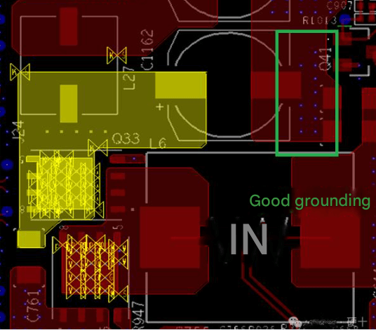
One fundamental strategy is to maintain a well-defined ground plane. A continuous ground plane acts as a reference point for signals and helps to minimize the loop area, thereby reducing the potential for electromagnetic coupling. Additionally, it provides a low-impedance path for return currents, which is vital for maintaining signal integrity.
Another key aspect of EMI management is the careful routing of signal traces.
High-speed signals should be routed with minimal length and should avoid sharp angles, as these can act as antennas, radiating unwanted electromagnetic energy. Differential signaling, where two complementary signals are routed together, can also be employed to reduce EMI. This technique helps to cancel out electromagnetic fields, as the fields generated by the two signals tend to negate each other.
Moreover, the use of decoupling capacitors is an effective method to suppress EMI.
These capacitors are placed close to power pins of integrated circuits to provide a local energy reservoir, which helps to stabilize voltage levels and reduce noise. Selecting the appropriate value and placement of decoupling capacitors is crucial for their effectiveness in mitigating EMI.
Shielding is another technique that can be employed to manage EMI.
By enclosing sensitive components or entire sections of the PCB in a conductive enclosure, it is possible to block external electromagnetic fields from interfering with the circuit. However, shielding can add to the cost and complexity of the design, so it should be used judiciously.
Furthermore, the choice of materials in PCB construction can influence EMI performance.
High-frequency laminates with low dielectric loss can help to reduce signal attenuation and minimize EMI. Additionally, the use of controlled impedance traces ensures that signal integrity is maintained, further reducing the potential for EMI.
In conclusion, managing electromagnetic interference in high-speed PCB design is a multifaceted challenge that requires a comprehensive understanding of both the sources of EMI and the strategies available for its mitigation. By implementing a combination of grounding, routing, decoupling, shielding, and material selection techniques, designers can significantly enhance the performance and reliability of high-speed PCBs. As technology continues to advance, the importance of effective EMI management will only grow, underscoring the need for ongoing education and adaptation in this critical area of electronic design.

